1. What Was Published
On August 18, 2026, Applied Materials published a technical blog by Jinho An, Ph.D., Senior Director in the company's Heterogeneous Integration business unit, and product marketing manager Kyla Zhao, laying out the process mechanisms behind three advanced packaging systems the company launched earlier this year: the Nokota VMax 2 electrochemical deposition (ECD) platform, the Opta Quad CMP platform, and the Producer Avila 2 PECVD system.
The launch itself was announced in June. What is new here is the failure-mode detail — specifically, which physical variation each tool is meant to suppress in high-bandwidth memory (HBM) manufacturing. The framing is that as packages add chiplets, denser interconnects and new bonding schemes, the limiting factors become die warpage, fine-pitch wiring formation and bonding precision rather than lithographic scaling.
2. Plating: Feature Density Distorts the Current Field
Electrochemical deposition forms both the through-silicon vias inside HBM DRAM dies and the microbumps that connect those dies. Applied identifies a specific mechanism that degrades it: variations in local feature density distort current distribution during deposition, producing non-uniform metal fill across the wafer.
The company's answer in Nokota VMax 2 is a capability it calls Adaptive Pattern Tuning (APT), which dynamically shapes the electric field during deposition to compensate for layout-driven variation. Applied states the system achieves void-free fill in TSVs smaller than 3 microns in diameter at aspect ratios deeper than 10:1, and that this precision maps directly onto stacking yield, reliability and electrical performance in high-layer-count stacks — because bump coplanarity is set by how uniformly the plating deposits.
3. CMP: Packaging Flatness Is a Different Problem Than Front-End Flatness
Applied places CMP at three separate points in the packaging flow — after TSV fill, after dielectric deposition, and after copper pad formation — and makes a distinction worth noting: compared with front-end applications, packaging CMP involves thicker films, longer polish times and tighter tolerances simultaneously.
That combination is what the Opta Quad platform is built around. The system continuously monitors wafer condition during polishing and makes real-time adjustments to hold thickness uniformity across the wafer, with flexible sequencing across the multi-step flow. The stated goal is stable planarization sustained over long polish times, because even minor surface variation reduces bond quality, yield and reliability downstream.
4. PECVD: Using Film Stress to Fight Warpage in Ultra-Thin Dies
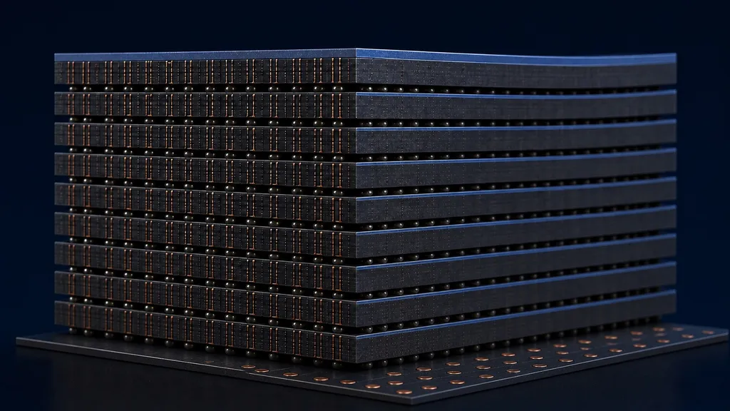
The most mechanically interesting item is the deposition angle on warpage. To add DRAM layers without exceeding package height limits, dies must get thinner — Applied puts today's HBM dies at roughly one twenty-fifth the thickness of conventional DRAM, which makes them far more vulnerable to stress, warpage and deformation. As stacks move from 12 to 16 layers and beyond, that compounds into misalignment, bonding defects and yield loss.
Producer Avila 2 addresses this by depositing engineered dielectric films that counteract warpage during TSV integration and stabilize the die through the rest of manufacturing. The concept is a stress-balanced film stack: the deposited layer is not merely an insulator but a mechanical counterweight, tuned so its intrinsic stress offsets the bow introduced by thinning and TSV integration.
This is a useful reminder of what PECVD process control actually buys in a packaging context. Film stress is a tunable knob — set by RF power, pressure, precursor ratio and temperature — and in ultra-thin die handling it becomes a yield parameter, not a specification footnote.
5. Why This Gets Harder at the Hybrid Bonding Transition
Applied is explicit that today's HBM designs still use thermocompression bonding with microbumps, and that hybrid bonding sits on the forward roadmap for greater interconnect density. Its position is that the three problems above do not go away at that transition — they tighten, because precision and uniformity requirements grow more stringent when copper pads must meet directly rather than through a solder joint.
The company points to Kinex, its integrated die-to-wafer hybrid bonding system developed with Besi, as the vehicle for that inflection. Kinex combines surface preparation, plasma activation, cleaning, metrology, alignment and bonding in a single platform, with reported throughput of 1,600 die placements per hour in high-volume production and scalability to six bonder modules. Applied also flags panel-based packaging and co-packaged optics as the next investment areas.
One caveat on reading this material: it is a vendor technical blog, not a peer-reviewed result or a customer yield disclosure. The mechanisms described — current-field distortion from pattern density, planarization drift over long polish times, stress-driven bow in thinned dies — are well established. The performance claims attached to each tool are the company's own.
6. NineScrolls Niche Angle
What makes this worth reading for a process or equipment engineer is that all three bottlenecks sit upstream of the bonder, in exactly the deposition and planarization steps that determine whether a bond succeeds. The plating side is the subject of our guide to TSV copper fill, which covers bottom-up superfill, additive chemistry and overburden CMP — the same physics Applied is addressing with field shaping, approached from the electrolyte side. For where these vias sit in the integration sequence, see our through-silicon via guide; for the backside thinning and reveal etch that make the dies thin enough to warp in the first place, see TSV reveal.
The CMP discussion maps almost one-to-one onto the pre-bond conditioning chain we walk through in surface preparation for Cu-Cu hybrid bonding — copper recess and dishing control, post-CMP cleaning, and the plasma activation window that converts the dielectric to a hydrophilic, bondable surface. Applied's point that packaging CMP means thicker films and longer polish times at tighter tolerances is precisely why that step is a yield gate rather than a formality, and why plasma activation is being integrated into the bonder itself.
The warpage argument connects to two places. Mechanically, bow and total thickness variation are what the wafers or dies must elastically overcome during the contact step described in our wafer bonding technologies guide — stress you fail to balance with the deposited film reappears as distortion and voids at the bond interface. Downstream, residual stress in a 16-high stack becomes the CTE-mismatch and interconnect fatigue problem covered in 3D packaging reliability and, thermally, in our look at 16-Hi HBM thermal and materials challenges. The interconnect crossover Applied is positioning for is laid out in hybrid bonding versus micro-bump.
For the equipment supply chain, the pattern is consistent with what we have tracked through 2026: value in advanced packaging keeps migrating toward the film and surface steps — conformal and stress-tuned PECVD, plating uniformity control, planarization stability, plasma activation — rather than the bonding step alone. Chamber-level control of deposition stress and uniformity is becoming a packaging yield lever, which is a genuinely different demand profile for deposition hardware than front-end scaling generated.
7. Sources
- Applied Materials — Tackling Key HBM and Advanced Packaging Bottlenecks for the AI Era (August 18, 2026)
- Applied Materials — Nokota VMax 2 ECD product page
- Applied Materials — Opta Quad CMP product page
- Applied Materials — Producer Avila 2 PECVD product page
- Applied Materials — Kinex Integrated Die-to-Wafer Hybrid Bonding System
- EE Times — Applied Materials, Besi Push Die-to-Wafer Hybrid Bonding Toward High-Volume Manufacturing
- Bits&Chips — Applied and Besi Unveil Integrated Die-to-Wafer Hybrid Bonder