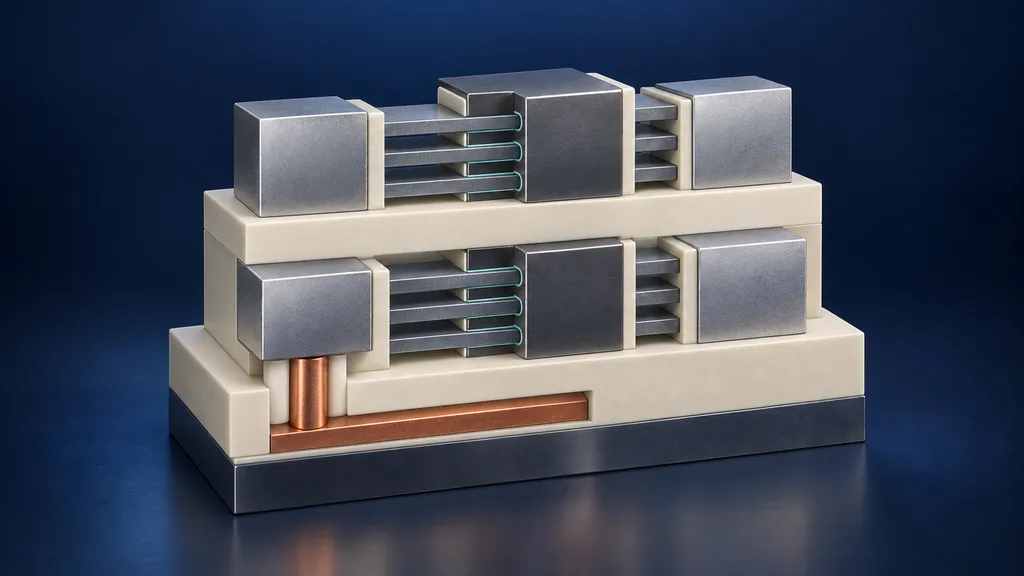
What imec Reported
On September 1, 2026, imec published Part 1 of a two-part report on advancing the complementary FET (CFET) roadmap, written by process integration engineer Cassie Sheng with Hiroaki Arimura and CMOS device technology director Naoto Horiguchi. It consolidates two process modules presented at the 2026 Symposium on VLSI Technology and Circuits.
The framing: gate-all-around nanosheet transistors scale to roughly the A10 generation and 5.5-track standard cells. From A7 onward, one path forward is CFET — stacking pMOS on nMOS — which imec says can take standard cells to 3T and extend classical CMOS logic to at least A3. The two modules reported are a backside contact scheme and a gate-stack integration scheme for multi-threshold-voltage tuning. Both are described as applicable to monolithic and sequential CFET alike.
Neither is a new tool announcement. Both are integration-sequence changes — where in the flow a film gets deposited, isolated, or removed — and both produce numbers.
The Backside Contact Fix: Add an Isolation Layer at the Front
Contacting the bottom device's source/drain junctions from the wafer backside beats frontside contacting on contact resistance, on the process window for top-device source/drain formation, on standard cell height, and on frontside BEOL routing congestion. It requires an extra module — backside dielectric isolation (BDI) — to electrically separate the source/drain epi from the substrate underneath.
The conventional approach forms that BDI structure entirely from the backside, near the end of the flow. imec names three consequences. The bottom SiGe:B source/drain is seeded during epi growth by both the bottom Si channel and the underlying Si substrate, so its volume varies. For the same reason it occupies space the contact metal cannot use, adding access resistance. And the scheme carries several yield-loss mechanisms for the backside contacts.
imec's answer is to form an additional BDI structure at the frontside, early. An extra Ge-rich SiGe layer is added to the Si/SiGe stack and later replaced with dielectric during the existing middle-dielectric-isolation module — so the step rides on infrastructure already in the flow rather than adding a new one. With the source/drain epi fully isolated from the substrate, the seeding problem disappears. A backside-formed BDI is still added downstream.
Reported results on a monolithic CFET test vehicle: bottom pFET drive current improved fivefold, access resistance fell from 1,753 Ω·µm to 378 Ω·µm, and bottom pFET survival yield rose from 45% to 85% against previously reported figures.
Bonding, Extreme Thinning, and the Backside Contact Etch
imec does not attribute the gain to the frontside isolation alone. It credits "an overall backside process optimization — involving wafer bonding, extreme wafer thinning, and backside contact etch" as also contributing to the pFET performance.
That sentence is the part worth reading twice. A backside contact module is, mechanically, the same class of problem as a backside via reveal: bond the device wafer, remove nearly all of the silicon behind it, then land a high-selectivity etch on a buried feature without overshooting into it. The process concerns are identical — total thickness variation after grind, endpoint control on the reveal etch, passivation integrity afterward. Our guide to backside thinning, reveal etch, and passivation covers that sequence in the TSV context it was developed for; the CFET backside contact borrows the same toolkit and tightens the tolerances, because what sits behind the thinned silicon is now a transistor junction rather than a copper via.
The bonding step is not incidental either. A wafer that will be thinned to the point of mechanical fragility has to be attached to something first, and the choice of bond determines the distortion the subsequent alignment has to absorb. The trade-offs across fusion, adhesive, eutectic, thermocompression, and hybrid routes are laid out in our wafer bonding technologies hub.
Dipole-Middle: Splitting the High-k Deposition in Two
The second module addresses threshold voltage tuning. Different devices on the same die want different Vt values, and the usual lever — varying gate metal composition and thickness to shift the effective work function — runs out of room between stacked nanosheets. The volume-free alternative is dipole tuning: insert a shifter metal such as lanthanum between the SiO₂ interlayer and the HfO₂ high-k, where it forms dipoles at the interface. Concentration sets the shift.
Two existing integration orders each fail in a different way. Dipole-last deposits La-oxide on top of the full HfO₂ layer and relies on a high-temperature anneal to drive it down to the HfO₂/SiO₂ interface — a thermal budget incompatible with CFET's low-temperature replacement metal-gate process. Dipole-first puts the shifter straight onto the SiO₂ and avoids the anneal, but patterning the La-oxide damages the SiO₂ interlayer beneath it and degrades the device.
The dipole-middle scheme splits the high-k deposition. A first thin HfO₂ layer goes down, then the shifter, then a mild anneal sufficient to diffuse it through that thin layer and lock it in. The thin HfO₂ doubles as a protective cap over the SiO₂ during shifter patterning. Unreacted shifter is removed, a second HfO₂ layer is deposited, and a second anneal follows. Total thermal budget stays below the dipole-last route, particularly when multiple shifter materials are integrated.
On a CFET test vehicle with only the top nFETs electrically accessible, the electrical data showed a small but consistent Vt reduction of about 30 mV against a reference where the La-oxide was removed before lock-in.
Note the process shape this creates: one gate dielectric, deposited in two separate passes with a patterning and anneal sequence in between, where the first pass has to be thin enough to let the shifter diffuse through and thick enough to survive as an etch stop over the interlayer. That is a conformality-and-thickness-control specification on a film only a few atomic layers thick, and the reason it is achievable at all is covered in our atomic layer deposition guide. The failure mode being designed around — patterning damage propagating into a layer beneath the one being etched — is the same ion-energy-versus-selectivity trade-off examined in PE versus RIE versus ICP-RIE plasma etching regimes.
Why Monolithic CFET Carries the Heavier Etch Burden
Both CFET flavors start from a vertical Si/SiGe stack. Monolithic CFET patterns and processes the whole stacked structure in one sequence — which, as imec puts it, requires considerable module development for the patterning, deposition, and selective removal of materials around and in between a high-aspect-ratio device structure. Sequential CFET patterns top and bottom devices independently with dedicated masks: individually simpler steps, but critical ones executed twice, plus two wafer flips that distort the wafer and challenge front-to-back alignment accuracy.
imec's read is that pending further progress in alignment accuracy, monolithic CFET offers the fastest path to industrial adoption. Read against tool requirements, that means the near-term burden lands on etch: removing one material selectively from between stacked channels inside a narrow, deep structure, without touching the channel silicon and without loading effects across the wafer. Decoupled ion energy and plasma density are what make that tractable, and the mechanism is set out in our ICP-RIE technology guide.
The work was carried out in the imec-hosted European NanoIC pilot line, jointly funded through the Chips Joint Undertaking and participating states. Part 2, covering DTCO studies of sequential CFET standard cell architectures and BEOL routability, has not yet been published.
NineScrolls Niche Angle
Plasma processing. The headline number here is a resistance figure, but the mechanism behind it is an etch and isolation sequence. Two etch demands stand out. The backside contact etch has to land on a transistor junction after extreme thinning, which is a selectivity and endpoint problem before it is a rate problem — the discipline described in our reveal etch guide. And the shifter patterning step in dipole-middle exists specifically because the earlier scheme's plasma damage reached a layer it should not have; the fix was to interpose a sacrificial-protective film rather than to soften the etch, which is a useful precedent for any lab patterning over a damage-sensitive interlayer.
Thin-film deposition. Splitting a HfO₂ gate dielectric into two ALD passes around a lanthanum insertion and a mild anneal turns high-k deposition into a multi-step sequence with an intermediate metrology and patterning stop. That raises the value of run-to-run thickness repeatability at sub-nanometre scale, because the first pass has two conflicting jobs at once. The same logic applies to the Ge-rich SiGe sacrificial layer in the frontside BDI scheme: it is deposited only in order to be selectively replaced later, so its composition tolerance is set by the removal chemistry, not by any electrical requirement.
Equipment supply chain. Nothing in this report requires a new tool class. It requires existing ICP etch, ALD, and bonding/thinning capability sequenced differently — which is exactly the kind of development that university and institute labs can contribute to without leading-edge fab capital. The open questions imec names are alignment accuracy after wafer flips, selectivity in confined high-aspect-ratio geometries, and low-thermal-budget dielectric integration. All three are addressable on 100–200 mm research platforms.
Caveat. These are conference disclosures on test vehicles, reported by imec. The dipole-middle result was measured on top nFETs only. There is no manufacturing yield, no node timeline beyond "most likely A7 onwards," and no production data.
Sources
- The imec Report: Advancing The CFET-Based Device Roadmap — Part I: Novel Integration Modules and Standard Cell Configurations, Cassie Sheng, Hiroaki Arimura and Naoto Horiguchi, Semiconductor Engineering, September 1, 2026
- Chip Industry Technical Paper Roundup: Sept. 1, Semiconductor Engineering, September 1, 2026
- Imec demonstrates functional monolithic CFET devices with stacked bottom and top contacts, imec press release, 2024
- Towards a process flow for monolithic CFET transistor architectures, imec Reading Room, 2023
- Performance boosters to scale monolithic CFET across multiple logic technology nodes, S. Yang et al., imec Reading Room, 2025
- Technical Highlights from the 2026 Symposium on VLSI Technology and Circuits