Dielectric Films
SiO2, SiNx, and SiON deposition for passivation, interlayer dielectric, optical, and MEMS workflows.
SiO2 / SiNx / SiONStress controlLow-temperature deposition
Equipment Platform
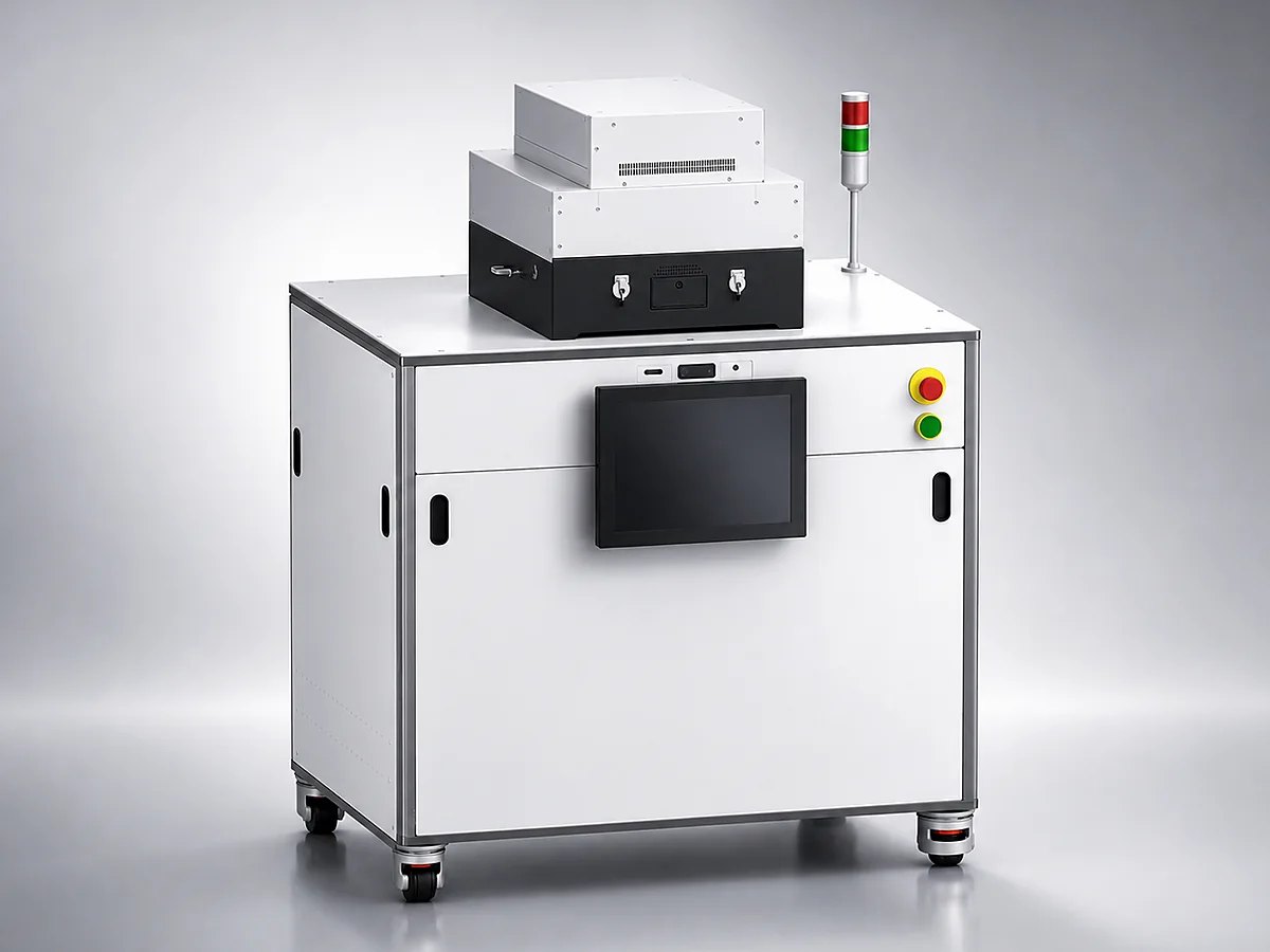
Low-temperature plasma-enhanced CVD for dielectric films, passivation layers, optical coatings, MEMS stacks, and research thin-film process development.
Wafer Size
4-12 in
RF Power
500-2000 W
Gas Lines
Up to 6
Temp Range
20 to 400 °C
Process-first configuration
PECVD selection starts with the target film, allowed thermal budget, stress target, refractive index, gas chemistry, deposition rate, and wafer handling requirements. The platform is configured around those process constraints rather than a fixed catalog setup.
SiO2, SiNx, and SiON deposition for passivation, interlayer dielectric, optical, and MEMS workflows.
a-Si:H and related plasma-deposited films for device research, sensors, and thin-film electronics.
SiC and optional DLC process configurations for barrier, encapsulation, and protective film development.
Core Process Windows
Plasma-assisted chemistry enables useful film growth at lower substrate temperatures than thermal CVD.
Single or dual-frequency RF configurations support stress and ion-bombardment tuning for MEMS and optical stacks.
Configurable gas delivery supports dielectric, semiconductor, and protective coating recipes in one platform family.
Technical Specifications
Review core platform capabilities for initial process planning. Our engineering team will confirm the final system configuration during quote review.
Applications
Passivation layers
Interlayer dielectrics
Optical coatings
MEMS membranes
Device encapsulation
Flexible electronics
Research evidence
Published work using the PECVD platform we represent · 5 papers
Dual-Zone Temperature-Modulated Growth of PtTe2/Ge Schottky Diodes for High-Speed Broadband Photodetection from Visible to 4.2 um
ACS Applied Materials & Interfaces 2026
Low temperature plasma deposited SiO2/organosilicon stacked film for transparent gate dielectric of InGaZnO thin film transistor
Thin Solid Films 2024
Selenization Mechanism of Nearly 4 in. Single-Oriented PtSe2 and PtSe2/n-Si/n+-Si 2D-3D PIN Wide-Spectrum Polarization Detectors
ACS Applied Materials & Interfaces 2025
Broadband and high-speed micro-scale PtSe2/Si 2D-3D PIN photodetector for on-chip polarization-encoded communication and imaging
Applied Surface Science 2026
In Situ Selenization Engineered Dual Schottky Heterojunctions: A Novel Architecture for High-Speed Broadband Photonic Communication Detector Arrays
Small 2025
Process evidence
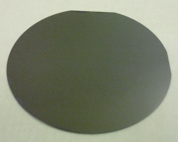
Four-inch whole-wafer SiO2 deposition achieved on the PECVD platform family.
Related Resources
FAQ
The PECVD platform supports common dielectric and semiconductor films including SiO2, SiNx, a-Si:H, SiC, SiON, and optional DLC process configurations.
PECVD uses plasma-assisted chemistry to enable film deposition at lower substrate temperatures, making it useful for passivation, encapsulation, MEMS, optical coatings, and temperature-sensitive research stacks.
The PECVD platform supports 4 inch to 12 inch wafers, 500 to 2000 W RF power at 13.56 MHz and/or 400 kHz, 20 to 400 °C temperature control, up to 6 gas lines, and <5% film uniformity.
Request a quote
Share your target film, substrate temperature limit, gas chemistry, wafer size, stress target, and timeline.