Dielectric Patterning
Controlled plasma etching for SiO2, SiNx, and related dielectric films used in research device stacks.
SiO2 / SiNxMask selectivityEndpoint ready
Equipment Platform
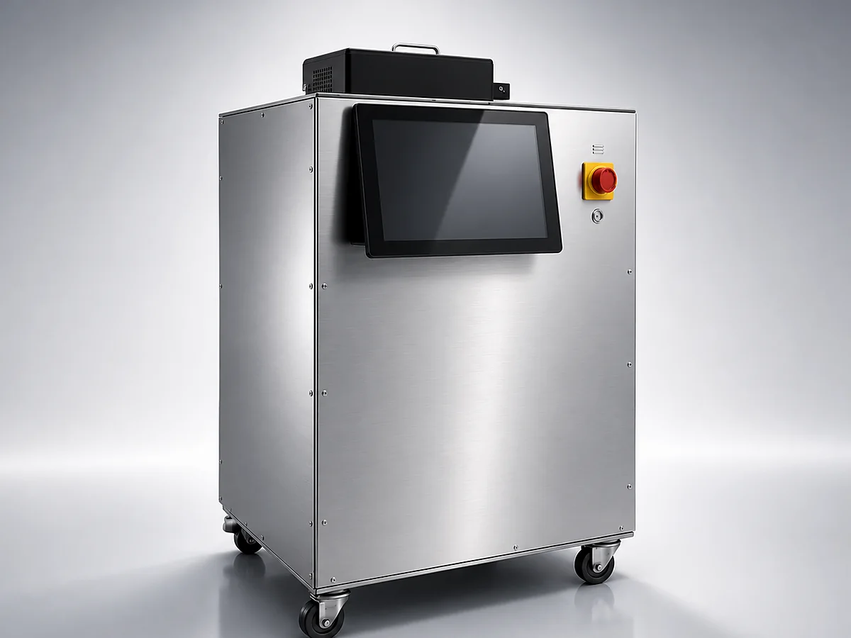
A general-purpose RIE etcher for reliable anisotropic plasma etching — dielectric patterning, polymer removal, surface activation, and device prototyping in university and R&D lab environments.
Wafer Size
4-12 in
RF Power
300-1000 W
Gas Lines
4 lines
Temp Range (option)
-70 to 200 °C
System overview · 72 seconds
Explore the system, look inside the chamber, and follow two oxygen-based process examples — from preparation to illustrative results.
Example configuration: 200 mm, 500 W RF, O₂/Ar. Final configuration is application-specific. 3D animations and application outcomes are illustrative.
Process-first configuration
RIE system selection starts with the target film, mask selectivity, ion directionality, allowable damage, pressure window, gas chemistry, and sample handling. These process requirements guide the platform configuration.
Controlled plasma etching for SiO2, SiNx, and related dielectric films used in research device stacks.
Oxygen and mixed-gas RIE workflows for photoresist, polymer films, surface cleaning, and device preparation.
General-purpose anisotropic etching for university labs and R&D teams building repeatable process windows.
Core Process Windows
RF-driven sheath control supports anisotropic etch profiles for moderate-aspect-ratio features.
Four gas lines support common fluorine, oxygen, argon, and mixed-gas research recipes.
Compact footprint, configurable loading, and automated recipe control suit repeated R&D workflows.
Technical Specifications
Review core platform capabilities for initial process planning. Our engineering team will confirm the final system configuration during quote review.
Applications
Semiconductor R&D
Dielectric patterning
Polymer removal
Surface activation
Device prototyping
MEMS fabrication
Research evidence
Published work using the RIE etching platform we represent · 16 papers
Large-area electrode deposition and patterning for monolayer organic field-effect transistors by vacuum-filtrated MXene
Advanced Electronic Materials 2024
Near-ideal van der Waals rectifiers based on all-two-dimensional Schottky junctions
Nature Communications 2021
Hidden vacancy benefit in monolayer 2D semiconductors
Advanced Materials 2021
Extremely vertical sidewall trench etching on silicon substrate and modelling etching using artificial neural network
Materials Research Express 2019
On-chip nonlocal metasurface for color router: conquering efficiency-loss from spatial-multiplexing
Light: Science & Applications 2025
Tuning metasurface dimensions by soft nanoimprint lithography and reactive ion etching
Advanced Photonics Research 2022
Multifunctional tendon-mimetic hydrogels
Science Advances 2023
Large-area silicon photonic crystal supporting bound states in the continuum and optical sensing formed by nanoimprint lithography
Nanoscale Advances 2023
Fluid Nanoforest Interfaces for Efficient Capture and In Situ MicroRNA and Protein Profiling of Tumor-Derived Extracellular Vesicles
ACS Nano 2025
High performance ZnS antireflection sub-wavelength structures with HfO2 protective film for infrared optical windows
Optics Express 2021
Synergistic-engineered van der Waals photodiodes with high efficiency
InfoMat 2022
Biomimetic microstructured diaphragms enable high-sensitivity and wide-dynamic-range fiber-optic microphones
Optics Express 2026
Metal-free synthesis of few-layer graphene films on insulating SiO2 and SiC substrates by chemical vapor deposition
Materials Research Express 2019
Composite Nanotube Arrays for Pesticide Detection Assisted with Machine Learning Based on SERS Effect
ACS Applied Nano Materials 2025
Wafer-Scale Graphene Growth on Si/SiO2 Substrates via Metal-Free Chemical Vapor Deposition
ACS Applied Nano Materials 2023
An Environment-Powered Soft Actuator Enabled by Water and Light Highly Absorptive Nanoforests
ACS Applied Nano Materials 2026
Process evidence
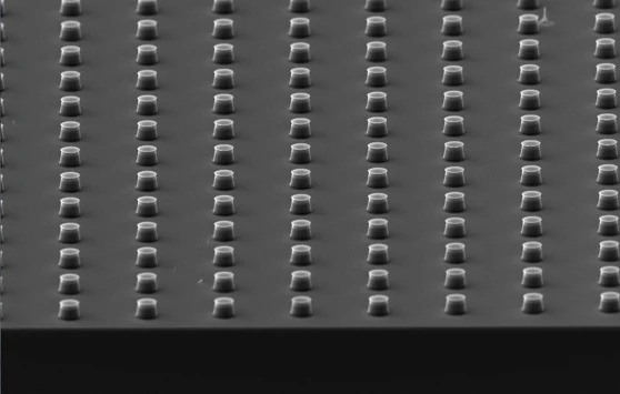
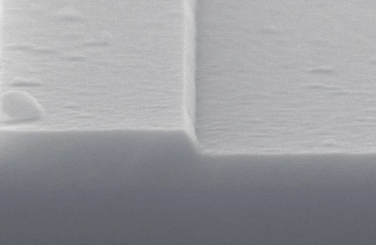
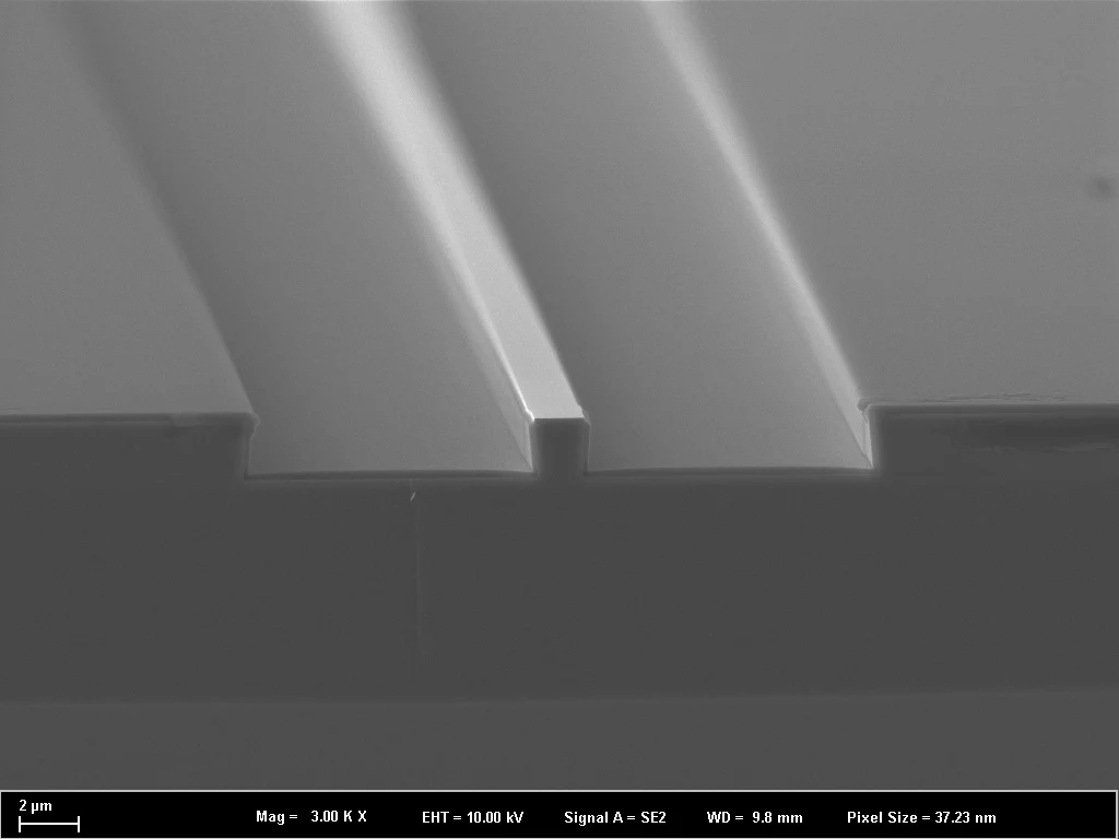
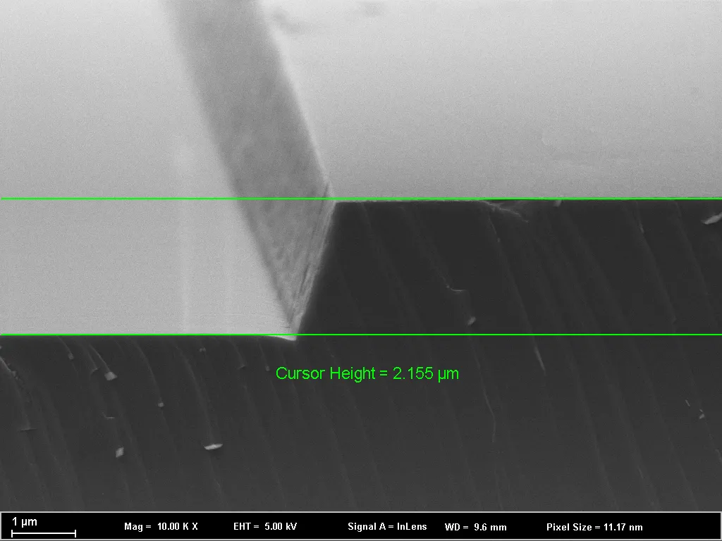
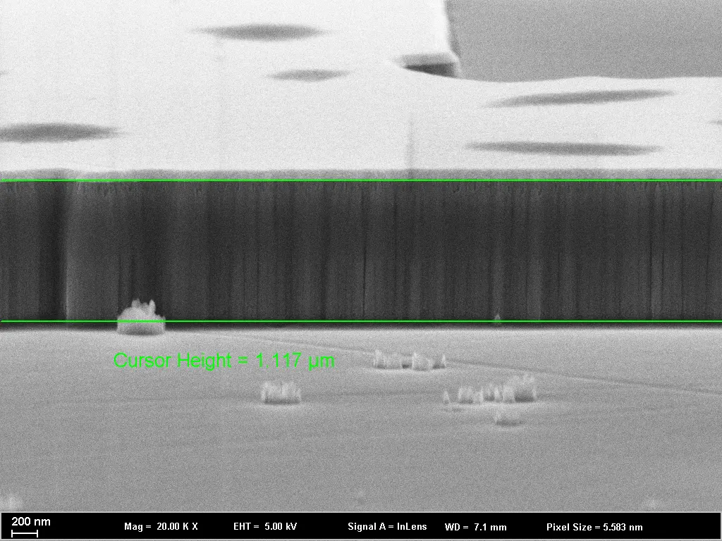
Representative SEM results achieved on the RIE platform family: silicon arrays and lens structures, InP ridges, and SiC etch profiles.
Related Resources
FAQ
The RIE platform supports silicon, silicon dioxide, silicon nitride, metals, polymers, and common research process stacks used in dielectric patterning, polymer removal, surface activation, and device prototyping.
RIE is a strong fit for general-purpose dry etching, moderate anisotropy, dielectric patterning, polymer removal, and cost-conscious R&D workflows. ICP-RIE is better when the process needs high-density plasma, higher aspect ratios, or independent control of plasma density and ion energy.
The RIE platform supports 4 inch to 12 inch wafers, 300-1000 W RF power at 13.56 MHz, 4 process gas lines, and an optional -70 to 200 °C wafer stage.
Request a quote
Share your target film, mask stack, wafer size, gases, process temperature, and lab timeline.