
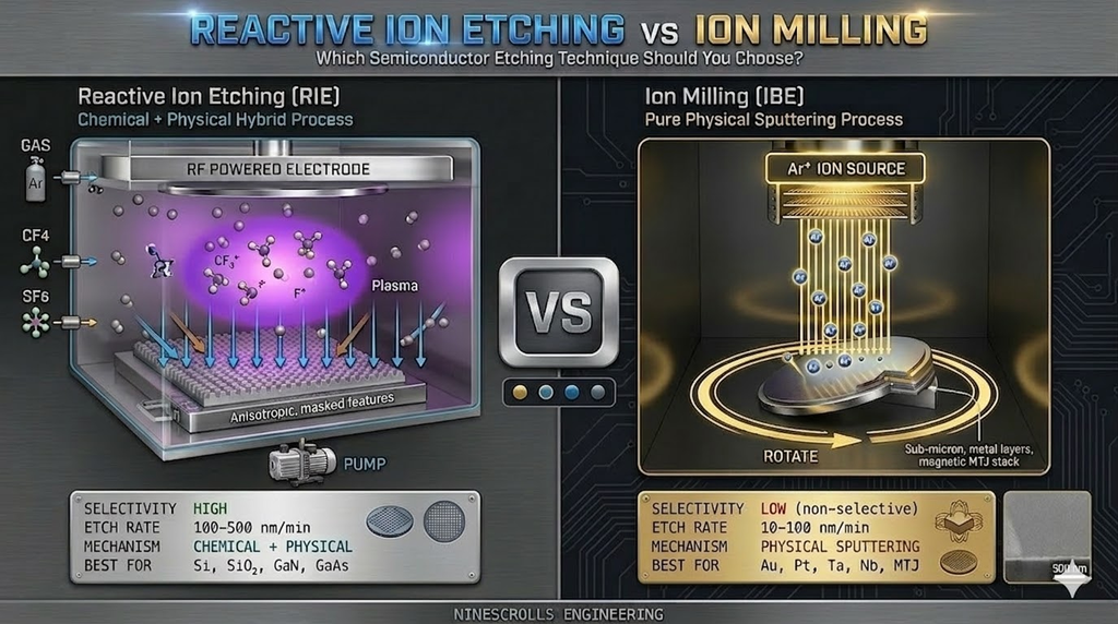
RIE vs Ion Milling: Two Different Material-Removal Mechanisms
This guide compares two fundamentally different material-removal mechanisms — chemically driven Reactive Ion Etching (RIE) and physically driven Ion Milling (also called Ion Beam Etching, IBE) — and shows when to choose each.
While both approaches rely on energetic ions to remove material, they differ significantly in their mechanisms, process control, and suitable applications. Understanding these differences is essential for selecting the right microfabrication etching method for your process requirements.
This guide provides quantitative process data, practical engineering insights, and a structured decision framework to help you choose between RIE, IBE, and hybrid approaches such as RIBE.
Is Ion Beam Milling Anisotropic? Quick Answer
Yes — ion beam milling (IBE) is highly anisotropic. The ion beam is collimated and arrives at the wafer with a tightly controlled angle (typically near-vertical, but tunable from 0° to 70°+ via a tiltable stage). Material removal happens almost exclusively along the ion trajectory, producing near-vertical sidewalls regardless of the substrate crystallography or chemistry. In practical terms IBE often delivers higher anisotropy than standard RIE because there is no isotropic chemical etch component, only directional sputtering. The trade-offs are slower etch rate, low material selectivity, and higher redeposition risk on sidewalls.
Sputter Etching vs RIE: Etch Rate Comparison
Sputter etching is purely physical (Ar⁺ ion bombardment, no reactive gas), while RIE combines physical bombardment with reactive chemistry. The chemistry term is what gives RIE its rate advantage on most semiconductor materials:
| Material | Sputter Etching (Ar⁺) | RIE (reactive chemistry) | Why the gap |
|---|---|---|---|
| Si | 10–30 nm/min | 200 nm – 5 µm/min (SF₆) | Volatile SiF₄ pumped away |
| SiO₂ | 15–40 nm/min | 50–600 nm/min (CHF₃/CF₄) | Fluorocarbon chemistry forms volatile SiF₄ + CO |
| Au, Pt | 20–50 nm/min | — (no volatile chloride/fluoride) | Noble metals require physical-only IBE |
| Co, NiFe (MTJ) | 20–40 nm/min | — (not viable in production) | No volatile etch product; IBE is industry standard |
| Photoresist | 50–200 nm/min | 200 nm – 5 µm/min (O₂) | Oxygen plasma forms CO, CO₂, H₂O |
Bottom line: for any material with a viable reactive chemistry, RIE is 5–100× faster than sputter etching. Sputter etching (and its directional cousin IBE) wins only when no volatile etch product exists — noble metals, magnetic stacks, complex oxides, and some compound semiconductors.
Working Principles
Reactive Ion Etching (RIE)
- Mechanism: Combines chemical reactions (from reactive gases like CF₄, SF₆, Cl₂, O₂) with ion bombardment from a plasma. The synergy between chemical and physical pathways yields etch rates significantly higher than either mechanism alone.
- Etch Directionality: Achieves anisotropic etching because ions are accelerated toward the substrate under an electric field, while reactive radicals provide selective chemical reactions.
- Control Parameters: Gas chemistry, RF power, pressure, and bias voltage allow fine‑tuning of etch rate, selectivity, and profile.
- Typical Etch Rates: Si in SF₆ plasma: 100–500 nm/min; SiO₂ in CHF₃/CF₄ plasma: 50–200 nm/min; GaAs in Cl₂/BCl₃ plasma: 200–800 nm/min (rates vary with RF power, pressure, and system configuration).
- Selectivity: Si:SiO₂ selectivity can exceed 30:1 under optimized SF₆/O₂ conditions; Si₃N₄:SiO₂ selectivity of 5–10:1 is achievable with CHF₃-based chemistries.
Key takeaway: RIE is best seen as a hybrid process: physical sputtering enhances anisotropy, while chemical reactions provide high selectivity. The combination of both mechanisms makes RIE the workhorse of semiconductor pattern transfer.

DRIE: Deep Reactive Ion Etching (Bosch Process)
An important variant of RIE is Deep Reactive Ion Etching (DRIE), particularly the Bosch process. DRIE uses alternating cycles of etching (typically SF₆) and passivation (C₄F₈) to achieve near-vertical sidewalls at extreme depths:
- High aspect ratio capability: Aspect ratios exceeding 50:1 are achievable, enabling structures from 1 µm to over 500 µm deep.
- Near-vertical sidewalls: Cyclic passivation protects sidewalls during each etch step, maintaining profile integrity.
- Key applications: MEMS inertial sensors (accelerometers, gyroscopes), Through-Silicon Vias (TSVs) for 3D IC integration, pressure sensor diaphragms, and microfluidic channels.
For applications requiring high-aspect-ratio structures, DRIE is often the technique of choice. See also our comparison of Cryogenic Plasma Etching vs. the Bosch Process for alternative deep-etch approaches.
Ion Milling (Ion Beam Etching, IBE)
- Mechanism: Purely physical sputtering process. An ion beam (typically Ar⁺) directly bombards the surface, physically ejecting atoms through momentum transfer.
- Etch Directionality: Controlled by the angle and energy of the ion beam, which can be normal incidence (vertical milling) or oblique (angled milling at 0°–85° from normal).
- Control Parameters: Beam energy (typically 300–1000 eV), incidence angle, and ion flux primarily determine etch rate and profile.
- Typical Etch Rates: Ar⁺ ion milling of most materials: 10–100 nm/min. Rates depend on beam energy, angle, and target material sputter yield — for example, Au sputters at roughly 2–3× the rate of SiO₂ under the same beam conditions.
Key takeaway: Ion Milling is essentially a "sandblasting" process at the nanoscale, offering precise directional control but no inherent chemical selectivity. Its universality — the ability to etch virtually any material — is its defining strength.

Advantages and Limitations
Reactive Ion Etching (RIE)
Advantages:
- High selectivity between materials (e.g., Si:SiO₂ > 30:1 with optimized chemistry).
- Can achieve vertical sidewalls with anisotropic control.
- Widely scalable for semiconductor production — RIE and ICP-RIE systems handle wafers from small research pieces to 300 mm production.
- High throughput (100–500 nm/min for common semiconductors), making it suitable for volume manufacturing.
Limitations:
- Potential polymer deposition and sidewall passivation complicate process control.
- Plasma‑induced damage (charging, contamination) can affect sensitive device layers.
- Limited to materials with suitable reactive gas chemistry — noble metals and many magnetic alloys lack effective RIE recipes.
- More complex system requirements (RF power, gas handling, vacuum).
Ion Milling (Ion Beam Etching, IBE)
Advantages:
- Works on any material (metals, insulators, hard‑to‑etch compounds) — no reactive chemistry required.
- Excellent for materials with no suitable reactive gas chemistry (e.g., Au, Pt, Ir, and magnetic alloys like CoFeB).
- Capable of angled etching for oblique features — incidence angle is continuously adjustable.
- Produces smooth sidewalls and minimal chemical residues.
- Decoupled ion generation and substrate processing reduces plasma-induced damage compared to RIE.
Limitations:
- Low etch rates (10–100 nm/min) limit throughput.
- Poor selectivity — everything sputters at broadly similar rates, making mask design critical.
- Can cause surface damage, amorphization, and redeposition of sputtered material on sidewalls.
- More expensive and complex beamline systems.
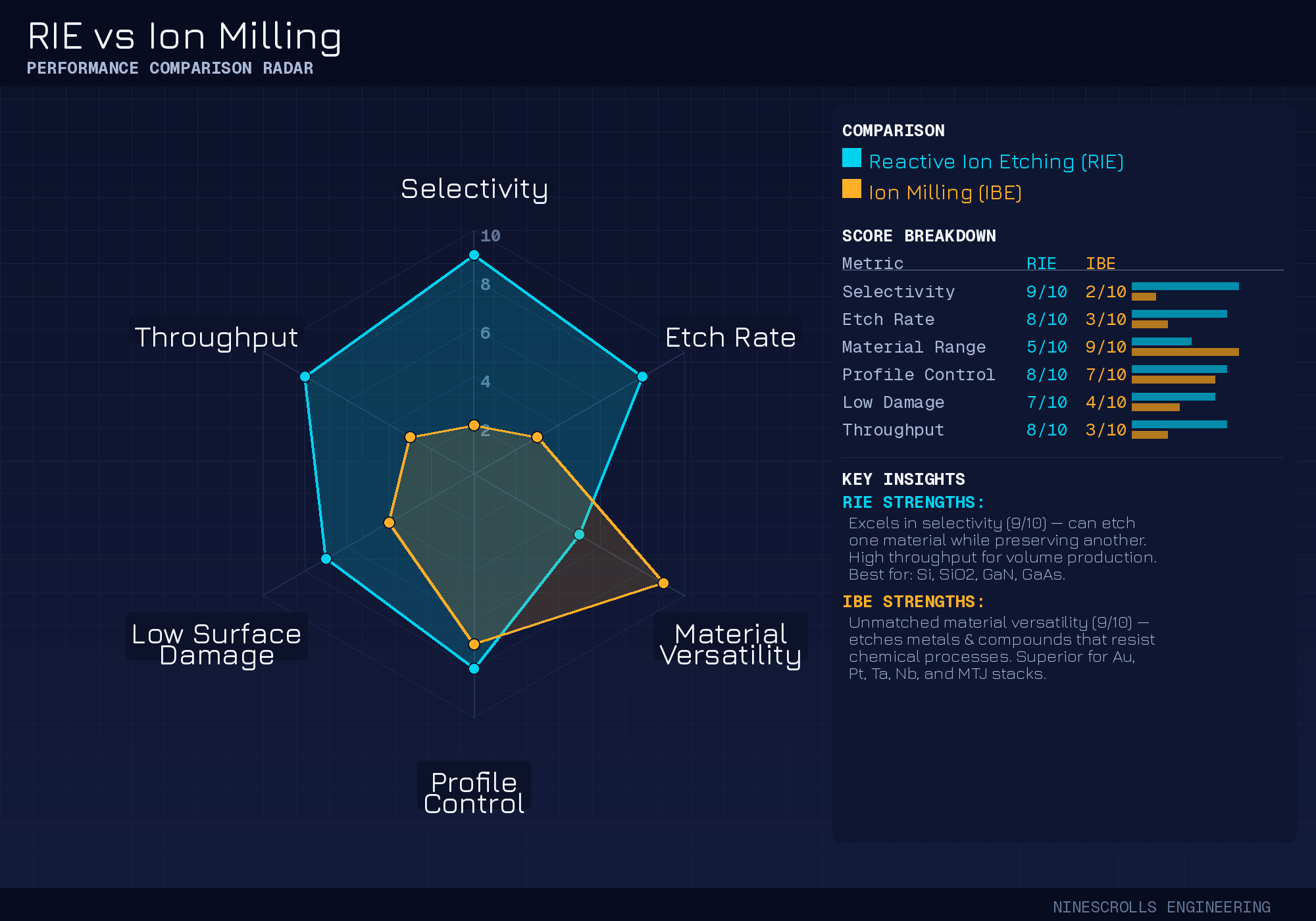
Etch Rate Comparison by Material
The following table provides typical etch rate ranges for common substrate and thin-film materials under representative RIE and Ion Milling conditions. Actual rates depend on system configuration, power, pressure, and beam parameters.
| Material | RIE Etch Rate (nm/min) | RIE Gas Chemistry | Ion Milling Rate (nm/min) |
|---|---|---|---|
| Si | 100–500 | SF₆, SF₆/O₂, Cl₂/HBr | 20–60 |
| SiO₂ | 50–200 | CHF₃/CF₄, C₄F₈/Ar | 15–40 |
| GaAs | 200–800 | Cl₂/BCl₃, SiCl₄ | 30–80 |
| GaN | 100–400 | Cl₂/BCl₃/Ar | 20–50 |
| SiC | 50–200 | SF₆/O₂, CF₄/O₂ | 10–30 |
| Au | — (no effective RIE chemistry) | — | 50–100 |
| Pt | — (no effective RIE chemistry) | — | 30–70 |
Note: All values are representative ranges. Actual etch rates depend on specific equipment, process parameters, and material quality. Ion milling rates are for Ar⁺ at 500–800 eV beam energy.
Process Challenges and Practical Solutions
Both RIE and Ion Milling present engineering challenges in practice. The following table summarizes common issues encountered in production and research, along with proven mitigation strategies.
| Challenge | Technique | Mitigation Strategy |
|---|---|---|
| Microloading — etch rate varies between dense and isolated features | RIE | Optimize gas flow distribution, adjust power density, use dummy pattern fill in low-density regions. With proper dummy structures, rate variation can be controlled to within ±5%. |
| ARDE (Aspect Ratio Dependent Etching) — etch rate decreases in deeper/narrower features | RIE / DRIE | Adjust etch/passivation cycle parameters, increase ion energy, optimize gas ratios. For MEMS deep trenches (AR > 20:1), progressively increasing SF₆ flow can compensate ARDE to maintain < 10% bottom rate deviation. |
| Redeposition — sputtered material redeposits on feature sidewalls | Ion Milling | Rotate sample stage continuously during milling, optimize incidence angle (typically 30°–60° oblique), improve beam scan uniformity. In MRAM MTJ patterning, adjusting Ar⁺ incidence to 45° with continuous rotation has been shown to reduce redeposition-induced short-circuit defects by approximately 80%. |
| Surface Damage & Amorphization — ion bombardment disrupts surface crystal structure | Ion Milling | Reduce beam energy to 300–500 eV range, apply post-etch thermal annealing to restore lattice order. In GaN HEMT gate etching, reducing beam energy from 800 eV to 400 eV has been reported to recover channel mobility to > 95% of the pristine value. |
These "problem + solution" insights reflect real-world process engineering experience. For more on plasma etch troubleshooting, see our guide to non-uniform etch chamber solutions.
Application Scenarios
- RIE is preferred when:
- Etching semiconductors (Si, GaAs, GaN, SiC) and dielectrics (SiO₂, Si₃N₄) where gas chemistry enables high selectivity.
- Fabricating CMOS, MEMS, TSVs, and photonic devices — applications where vertical profiles and throughput are critical, often paired with downstream HDP-CVD dielectric gap-fill.
- High aspect ratio patterns are required — standard RIE handles up to ~5:1 AR, while ICP-RIE and DRIE extend this to 20:1 and beyond.
If you are looking for a flexible RIE or ICP system for your lab, NineScrolls offers a full range of solutions from R&D to small-batch production. View RIE Systems · View ICP Systems
- Ion Milling is preferred when:
- Etching metals (Au, Pt, Ta, Nb, Ir, etc.) or compound materials resistant to RIE chemistry.
- Pattern transfer in magnetic devices (MRAM, spintronics) where the magnetic stack lacks viable reactive etch recipes.
- Research‑scale fabrication requiring directional control at oblique angles for custom etch profiles.
- Removing thin films or "cleaning" surfaces without chemical residues.
For precision patterning of metal thin films or magnetic materials, our IBE/RIBE systems support multi-angle milling and endpoint detection. View IBE/RIBE Systems
Decision Framework
| Factor | Reactive Ion Etching (RIE) | Ion Milling (IBE) |
|---|---|---|
| Etch Mechanism | Physical + Chemical (Plasma) | Physical Sputtering (Ion Beam) |
| Selectivity | High — tunable via gas chemistry (e.g., Si:SiO₂ > 30:1) | Low — non‑selective physical sputtering |
| Etch Rate | 100–500 nm/min (material dependent) | 10–100 nm/min (material dependent) |
| Throughput | High — suitable for volume production | Low — primarily R&D and specialty processes |
| Material Scope | Semiconductors, dielectrics (requires suitable gas chemistry) | Any material — metals, insulators, compounds |
| Profile Control | Vertical sidewalls via anisotropic plasma | Beam-angle dependent — continuously adjustable |
| Damage/Residue | Plasma damage, possible polymer residue | Surface amorphization, redeposition |
| Best Use Case | High‑volume semiconductor & MEMS processes | Metals, magnetic devices, research‑scale patterning |
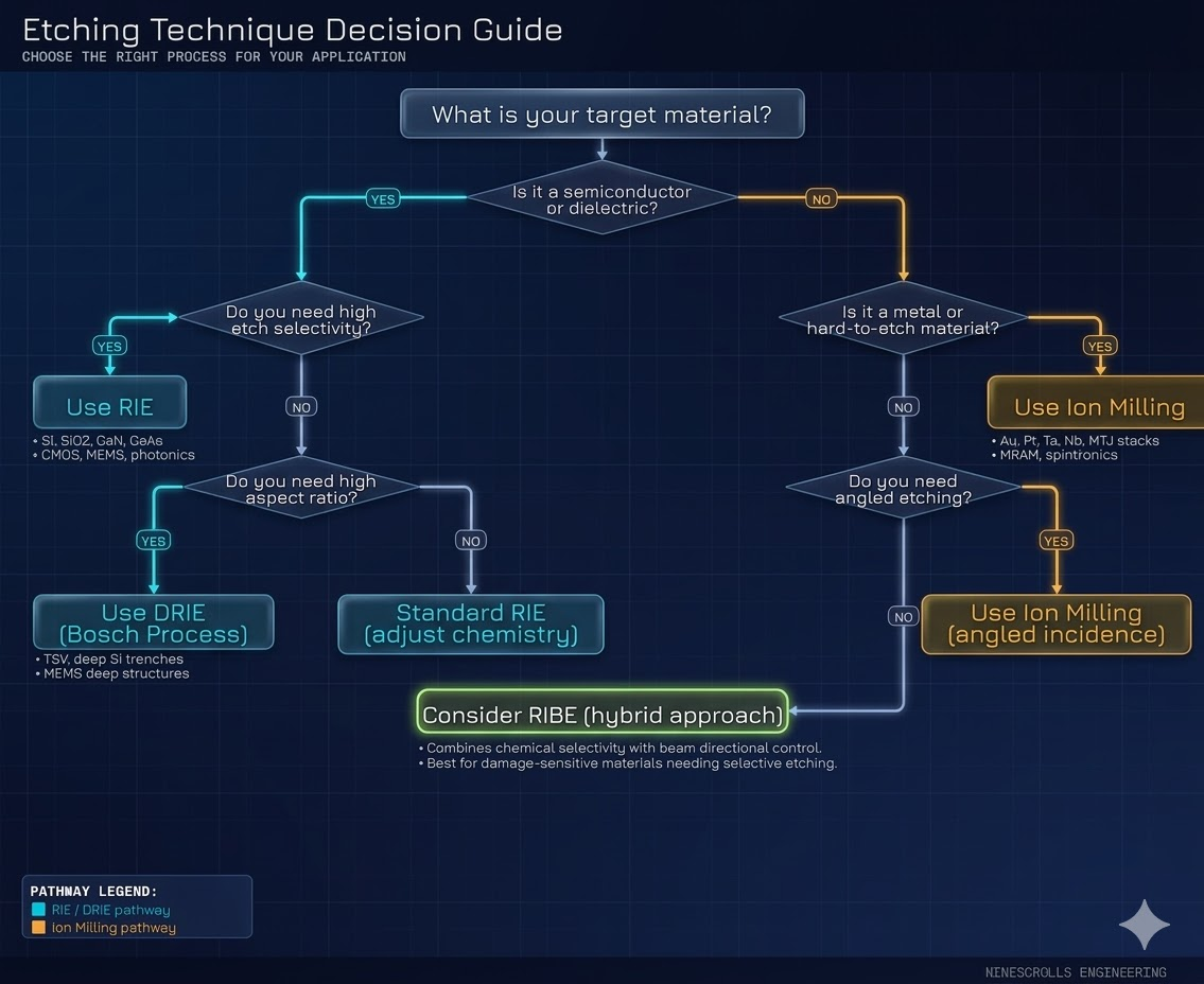
Beyond RIE and IBE: Hybrid Approaches (RIBE)
Reactive Ion Beam Etching (RIBE) bridges the gap between RIE and IBE by introducing reactive gases (such as O₂, Cl₂, or CHF₃) into the ion beam source. This hybrid approach combines the chemical selectivity of RIE with the directional beam control of IBE, offering unique advantages for demanding applications.
RIBE is particularly well-suited for scenarios where:
- Chemical selectivity is needed, but the substrate or device layers are sensitive to the plasma-induced damage inherent in conventional RIE.
- Precise angle control is required alongside some degree of material-selective etching.
- Complex multi-material stacks (e.g., magnetic tunnel junctions, photonic waveguides) need to be patterned with minimal cross-contamination.
Four-Way Comparison: RIE vs. Ion Milling vs. DRIE vs. RIBE
| Dimension | RIE | Ion Milling (IBE) | DRIE | RIBE |
|---|---|---|---|---|
| Etch Rate | 50 nm – 5 µm/min | 10–100 nm/min | 5–20 µm/min (Si) | 100–500 nm/min |
| Anisotropy | High | Very High (collimated beam) | Very High (passivation cycles) | Very High (collimated beam) |
| Selectivity | High (material-dependent) | Low (~1:1 to 3:1) | Very High (80:1 to mask) | Moderate — tunable via reactive gas |
| Aspect Ratio | 3:1 to 10:1 | ≤ 5:1 | ≥ 50:1 | ≤ 5:1 |
| Plasma Damage | Moderate — direct plasma exposure | Low — decoupled beam | Moderate — direct plasma exposure | Low — decoupled beam |
| Directional Control | Vertical (field-driven) | Full angle control (0–70°) | Vertical (field-driven) | Full angle control |
| Material Range | Semiconductors, dielectrics | Any material (incl. noble metals, magnetics) | Silicon (and a few III-Vs) | Broad — incl. some metals with reactive assist |
| Redeposition | Low (volatile etch products) | High risk | Low (volatile SiF₄) | Reduced — reactive gas forms volatile by-products |
| Best For | CMOS, dielectric patterning | MTJ, magnetics, noble metals | MEMS, TSV, deep Si trenches | Damage-sensitive metals & oxides |
NineScrolls' RIBE systems combine chemical enhancement with ion beam directional control, making them especially effective for damage-sensitive materials that require selective etching.
Conclusion
Both Reactive Ion Etching (RIE) and Ion Milling (IBE) are indispensable in microfabrication, but their strengths lie in different domains:
- If you need high selectivity, vertical profiles, and production-scale throughput, RIE (including ICP-RIE and DRIE variants) is the natural choice for semiconductors and dielectrics.
- If you need to etch metals, magnetic materials, or compounds that resist reactive chemistries — or require precise angular control — Ion Milling is the technique of choice.
- For applications requiring both selectivity and low damage, RIBE offers a compelling hybrid solution.
In practice, many advanced research labs and fabs integrate multiple etching technologies, selecting the optimal technique for each layer and material in their process flow.
Not sure which etching technique fits your process?
Whether you are etching metals with IBE or patterning semiconductors with RIE, our engineering team can help you evaluate materials, geometries, and throughput requirements to recommend the right solution.
Discuss Your RequirementsFAQ
Q1: Is ion beam milling anisotropic?
A: Yes — ion beam milling (IBE) is highly anisotropic because the ion beam is collimated and arrives at the wafer with a tightly controlled angle (typically near-vertical, but tunable from 0° to 70°+ via a tiltable stage). Material removal happens almost exclusively along the ion trajectory, producing near-vertical sidewalls regardless of the substrate's crystallography or chemistry.
Q2: What's the etch rate difference between sputter etching and reactive ion etching?
A: Sputter etching (purely physical, no reactive gas) typically runs at 5–50 nm/min depending on material, while RIE rates range from 50 nm/min up to several µm/min because reactive radicals form volatile byproducts that are pumped away. The gap is largest on materials with good chemical etch paths (Si, SiO₂) and smallest on inert materials like noble metals where RIE loses its chemical advantage.
Q3: When should I choose IBE over RIE?
A: Choose IBE when (1) your material has no good reactive chemistry — magnetics (Co, NiFe, MTJ stacks), noble metals (Pt, Au), or compounds like permanent magnets; (2) you need angular control for facet engineering or undercut shaping; or (3) the substrate is damage-sensitive and you can tolerate slower rates. Stay with RIE/ICP-RIE for production-throughput etching of Si, SiO₂, Si₃N₄, III-V semiconductors, and most photoresist-masked patterning.
Q4: Can RIE etch metals?
A: Some metals — Al, Ti, W, Mo, Ta — etch well in chlorine-based RIE plasmas (Cl₂/BCl₃) because they form volatile chlorides. Other metals (Au, Pt, Cu, Ni, Co, Fe) lack volatile etch products under typical RIE conditions and are usually patterned by ion milling, lift-off, or wet etch instead. Cu can be etched by some emerging plasma chemistries but is rarely done in production.
Q5: Is ion milling end-pointed?
A: IBE end-point detection is harder than RIE because there are no chemical reaction products to monitor via OES. The standard approaches are SIMS (mass spectrometry of sputtered species, very accurate but adds tool cost), interferometry on transparent stacks, and time-based recipes calibrated against a witness wafer. For MTJ etching, SIMS-based end-point is the production standard.
References
- Coburn, J. W. "Plasma-assisted etching." Plasma Chemistry and Plasma Processing, 2(1), 1–41 (1982). doi:10.1007/BF00566856
- Sigmund, P. "Theory of sputtering. I. Sputtering yield of amorphous and polycrystalline targets." Physical Review, 184(2), 383 (1969). doi:10.1103/PhysRev.184.383
- Harper, J. M. E. "Ion beam etching." In Thin Film Processes, Academic Press, 175–206 (1978). ISBN 978-0125219501.
- Flamm, D. L. & Donnelly, V. M. "The design of plasma etchants." Plasma Chemistry and Plasma Processing, 1(4), 317–363 (1981). doi:10.1007/BF00565992
- Wu, B., Kumar, A. & Pamarthy, S. "High aspect ratio silicon etch: A review." Journal of Applied Physics, 108(5), 051101 (2010). doi:10.1063/1.3474652
- Lee, S. et al. "Ion beam etching of MTJ nanopillars for high-density MRAM." Journal of Vacuum Science & Technology B, 36(3), 032201 (2018). doi:10.1116/1.5020731
- Laermer, F. & Schilp, A. "Method of anisotropically etching silicon." U.S. Patent 5,501,893 (1996). (Bosch process patent)
- Gottscho, R. A., Jurgensen, C. W. & Vitkavage, D. J. "Microscopic uniformity in plasma etching." Journal of Vacuum Science & Technology B, 10(5), 2133–2147 (1992). doi:10.1116/1.586180