Applications
Silicon photonics probing at wafer level
Photonic chips have to be tested before dicing just like electronic ones — but the signal is light. Wafer-level photonic testing adds fiber alignment stages next to electrical probes, so light can couple into on-chip waveguides while the device is driven and read electrically.
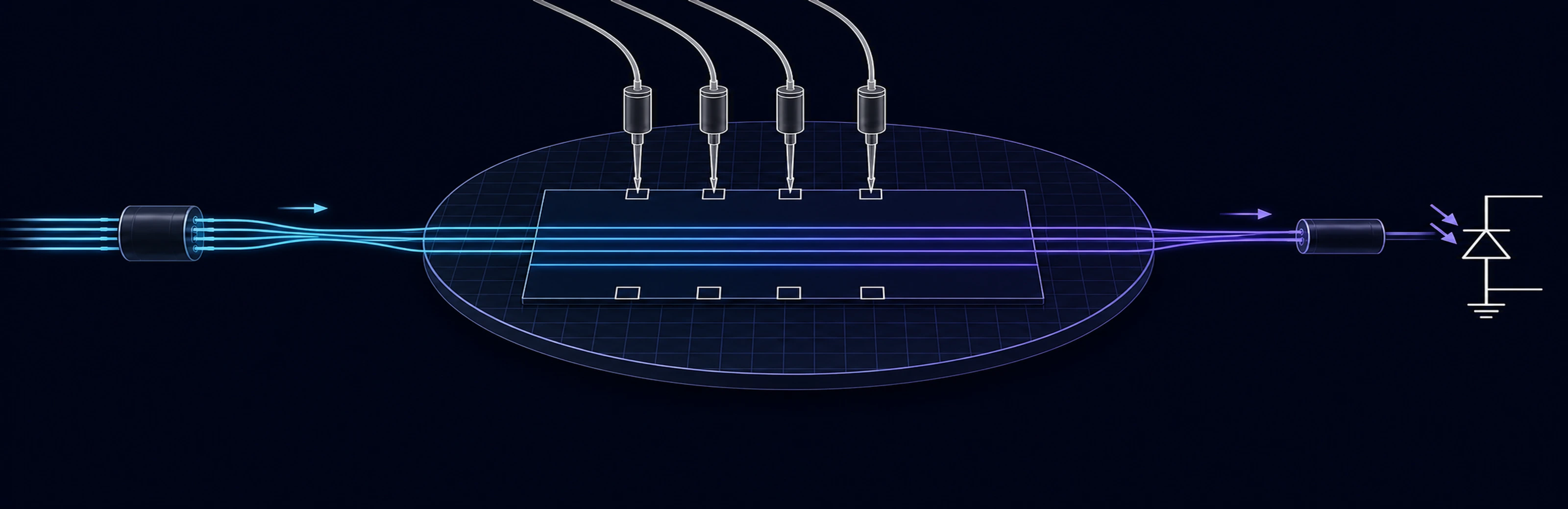
Define the coupling method
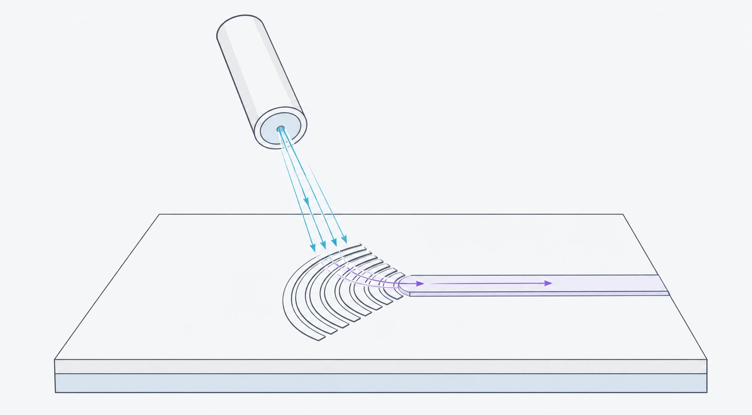
Vertical / grating coupling
Vertical fiber-to-waveguide coupling through grating structures
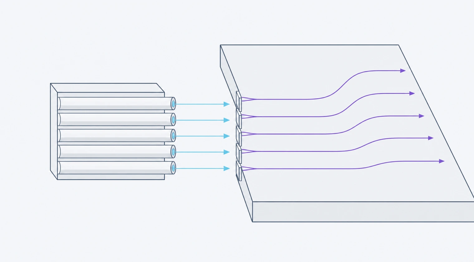
Edge coupling
Wafer-level alignment and coupling between fiber arrays and chip-edge waveguides
Plan the mixed-signal interfaces
- Optical
- Couple light into and out of the device.
- DC
- Apply bias and read electrical response.
- RF
- Drive and measure high-frequency electrical signals.
Choose the automation path
Semi-automatic path
- V Series — Automatic Probe Stations
- Listed
- X Series — Semi-Automatic Probe Stations
- Listed
- A Series — Fully Automatic Mass Production Probe Stations
- Not indicated in supplied brochure
Fully automatic path
- V Series — Automatic Probe Stations
- Listed
- X Series — Semi-Automatic Probe Stations
- Not indicated in supplied brochure
- A Series — Fully Automatic Mass Production Probe Stations
- Listed
Manufacturer-documented system capabilities
- Probe-station platform
- Built on semi-automatic and fully automatic probe stations
- Test-mode switching
- Single-fiber / array and vertical / edge configurations
- Coupling modes
- Edge / wafer-level edge / vertical coupling
- Grating coupling
- Listed for V, X, and A series in the supplied brochure
- Fiber and positioning calibration
- Automated fiber and positioning calibration
- Positioning platforms
- High-precision six-axis coupling platforms and piezoelectric ceramics
- Probe Z-axis monitoring
- Real-time monitoring of probe Z-axis height
- Instrument integration
- Customizable testing with mainstream instrument integration
- Edge-coupling alignment
- Automated alignment for chip-edge coupling
- Edge-coupling fiber clamps
- Interchangeable clamps for single-fiber and fiber-array coupling
- Wafer-level edge coupling
- Wafer-level alignment and coupling between fiber arrays and chip-edge waveguides
- Vertical coupling
- Vertical fiber-to-waveguide coupling through grating structures
- Silicon photonics test software
- Automated alignment, sub-die management, optical-alignment verification, calibration-wafer verification, wafer training, and measurement-position training
- PTS™ Integrated Test System Software
- Programmable-instrument integration, mainstream engineering and production prober support, customizable test functions, multi-site parallel testing, data integration and analysis, custom reports, and open export interfaces
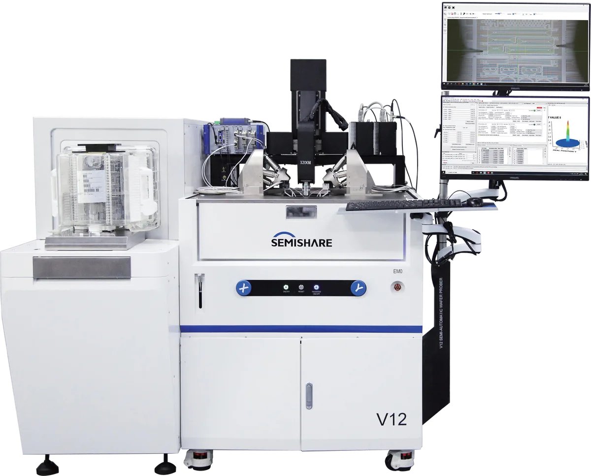
Coupling and calibration compatibility
Silicon photonics compatibility table
| Capability | V Series | X Series | A Series |
|---|---|---|---|
| Automatic calibration at multiple temperatures | Listed | Listed | Listed |
| Die-level edge coupling | Listed | Listed | Not indicated in supplied brochure |
| Wafer-level edge coupling | Listed | Listed | Listed |
| Vertical coupling | Listed | Listed | Listed |
| Grating coupling | Listed | Listed | Listed |
A blank cell in the manufacturer brochure is shown as “Not indicated in supplied brochure”. It records only what the supplied document lists, not a statement that a capability is unavailable.
The probe station selection hub covers base-platform decisions. This compatibility table records which SEMISHARE product lines the manufacturer brochure lists each capability for. NineScrolls handles US procurement and support.
Building a photonic test setup?
Tell us your coupling method, wavelength range, and electrical probing needs — we will scope a configuration and quote with US delivery and support.