Metal Films
DC magnetron workflows for conductive films, contact layers, seed layers, and research metallization stacks.
DC sputteringConductive targetsMetallization
Equipment Platform
Physical vapor deposition for metal, dielectric, nitride, oxide, magnetic, optical, and compound thin films using configurable DC/RF magnetron sputtering sources.
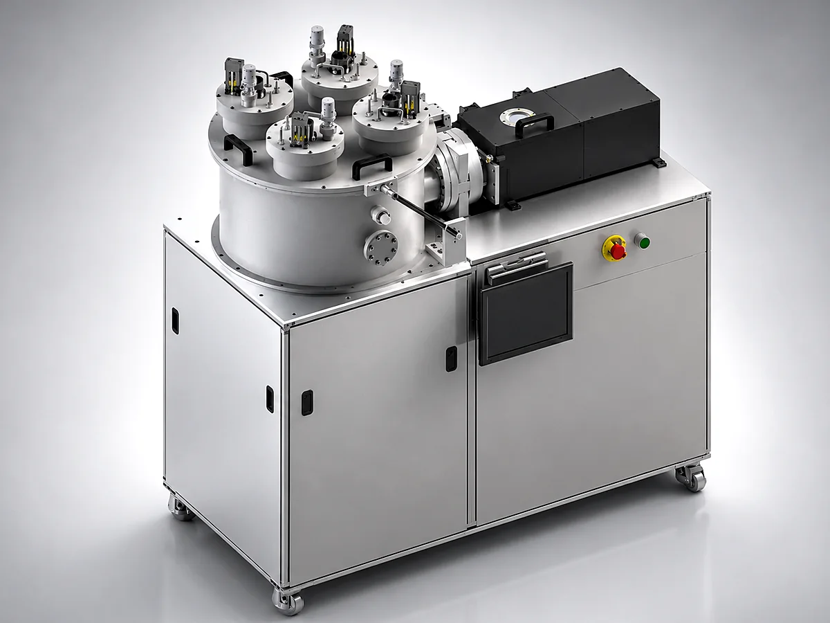
Wafer Size
4-12 in
Targets
2-6 configurable
Base Pressure
<5x10^-7 Torr
Uniformity
< +/-5%
Process-first configuration
Sputter selection starts with target materials, DC or RF power mode, reactive gas needs, base pressure, substrate temperature, wafer size, uniformity target, and whether the process needs multilayer or co-sputtering capability.
DC magnetron workflows for conductive films, contact layers, seed layers, and research metallization stacks.
Reactive oxygen or nitrogen process windows for oxide and nitride films with controlled stoichiometry.
Configurable target positions support multilayer films, alloy development, magnetic stacks, and co-sputtering workflows.
Core Process Windows
Two to six independently configurable targets support single-material, multilayer, alloy, and co-sputtered film development.
Power-mode flexibility supports conductive and insulating target materials across metal, oxide, nitride, and optical films.
Low base pressure and configurable substrate temperature help tune density, adhesion, stress, and film morphology.
Technical Specifications
Review core platform capabilities for initial process planning. Our engineering team will confirm the final target count, power supplies, gases, and substrate heating during quote review.
Applications
Metal contacts
Magnetic films
Optical coatings
Compound semiconductors
Protective coatings
Multilayer stacks
Research evidence
Published work using the magnetron sputtering platform we represent · 2 papers
Microalloying induced stable welded interfaces for highly reversible zero-excess sodium metal batteries
Energy & Environmental Science 2024
Tuning the Catalytic Selectivity Toward C2+ Oxygenate Products by Manipulating Cu Oxidation States in CO Electroreduction
ACS Applied Materials & Interfaces 2024
Related Resources
FAQ
The Sputter platform supports metal, oxide, nitride, magnetic, compound semiconductor, optical, and protective thin-film workflows depending on target configuration and DC, RF, or reactive sputtering mode.
Choose sputtering for broad PVD material compatibility, metal and magnetic films, conductive coatings, optical stacks, and multi-target or co-sputtering workflows. ALD is stronger for atomic-scale conformality, while PECVD is stronger for high-rate low-temperature dielectric films.
The Sputter platform supports 4 inch to 12 inch wafers, 2 to 6 independently configurable targets, substrate temperature from water-cooled to 1200 °C, base pressure below 5x10^-7 Torr, and < +/-5% film non-uniformity.
Request a quote
Share your target materials, wafer size, power mode, substrate temperature, pressure requirements, reactive gases, and timeline.