Dep/Sputter Gap-Fill
High-density plasma deposition plus controlled ion sputtering helps prevent top pinch-off and supports void-free fill strategies.
Dep/sputter balanceVoid suppressionD/S tuning
Equipment Platform
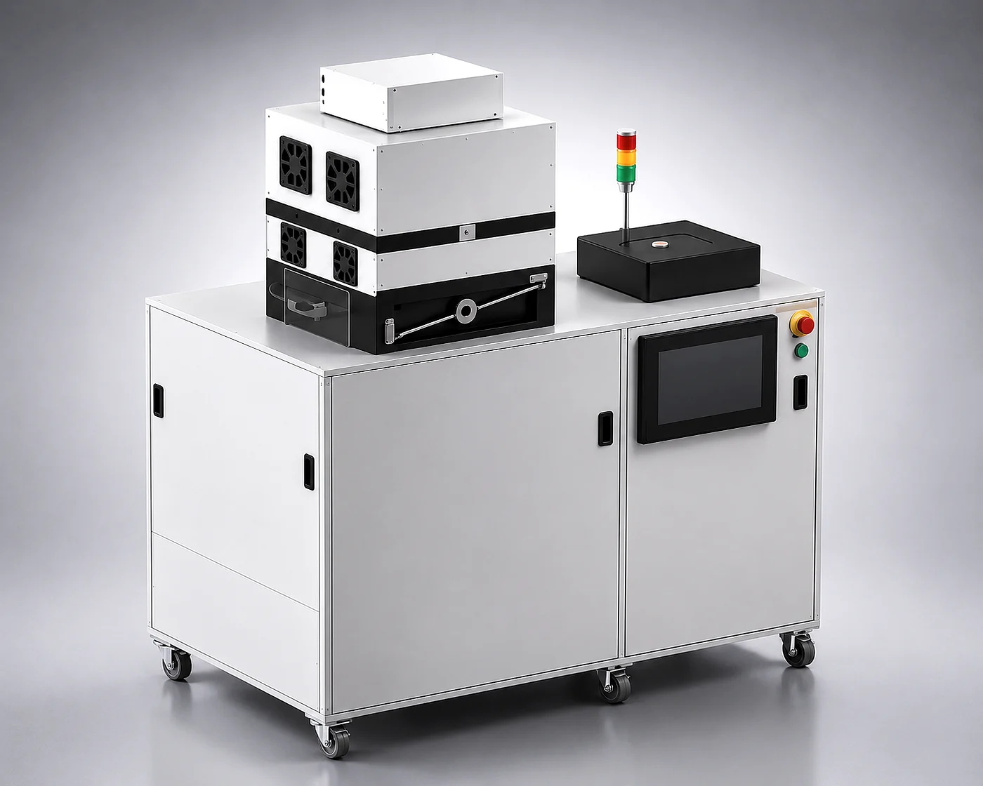
High-density plasma CVD for dense dielectric films, void-free trench fill, STI, IMD, PMD, and advanced packaging process development.
Wafer Size
4-12 in
Source RF
1000-3000 W
Bias RF
300-1000 W
Gas Lines
6
Process-first configuration
HDP-CVD selection starts with feature aspect ratio, target dielectric, D/S ratio, source power, bias power, gas chemistry, wafer temperature, film stress, and whether the process needs blanket dense films or true gap-fill performance.
High-density plasma deposition plus controlled ion sputtering helps prevent top pinch-off and supports void-free fill strategies.
Process windows support SiO2, Si3N4, SiON, SiC, low-k, and doped silicate glass film development.
20 to 200 °C operation supports research flows where dense films and plasma-assisted fill are needed without high thermal exposure.
Core Process Windows
The primary process target is void suppression in trenches, vias, and dense topography where conformal deposition alone can close the opening too early.
Independent source and bias RF ranges let engineers tune plasma density, ion energy, resputtering, and net deposition behavior.
HDP-CVD is configured for dense dielectric films with <5% uniformity and process windows for stress, wet etch rate, and dielectric quality.
Technical Specifications
Review core platform capabilities for initial process planning. Our engineering team will confirm the final gas chemistry, source, bias, loading, and chamber options during quote review.
Applications
STI gap-fill
IMD / PMD dielectrics
Advanced packaging dielectrics
TSV isolation workflows
MEMS cavity sealing
Silicon photonics cladding
Research evidence
Related Resources
Resource
Process principles, gap-fill behavior, PECVD and ALD comparison, and equipment selection
Resource
STI, IMD, PMD, advanced packaging, D/S ratio optimization, and void-free fill strategies
Resource
Deposition technology comparison for thin-film process planning
FAQ
HDP-CVD is used for high-density dielectric films and void-free gap-fill in high-aspect-ratio features, including STI, IMD, PMD, TSV-related dielectrics, MEMS cavity sealing, and advanced packaging workflows.
HDP-CVD combines plasma-enhanced deposition with ion-assisted sputtering. That dep/sputter balance keeps feature openings clear during deposition, improving gap-fill where standard PECVD can pinch off and form voids.
The HDP-CVD platform supports 4 inch to 12 inch wafers, 1000 to 3000 W source RF, optional 300 to 1000 W bias RF, 20 to 200 °C operation, a 6-line gas system, and <5% uniformity.
Request a quote
Share your target film, feature geometry, aspect ratio, wafer size, gas chemistry, source and bias requirements, and timeline.