Semiconductor
Etching, deposition, and plasma treatment for device R&D and pilot-line process modules.
Industrial Precision. Scientific Confidence.
Semiconductor process equipment engineered for research and advanced manufacturing, including ICP-RIE, RIE, PECVD, ALD, sputtering, and thin-film processing systems.
Trusted by universities, national laboratories, and semiconductor innovators.
12+
Equipment Platforms
50+
Supported Processes
20+
Research Applications
2-Year
Standard Warranty
Process Capability
Engineers do not shop by catalog first. They look for a stable process window, compatible materials, and equipment that can reproduce the result.
View all processesHigh-aspect-ratio etch workflows for MEMS, TSV, and advanced device prototyping.
Core processConformal and plasma-enhanced films for dielectrics, barriers, passivation, and device stacks.
Active process map
Equipment
Applications
Resources
Applications
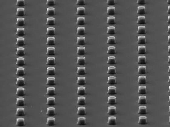
Silicon array pattern
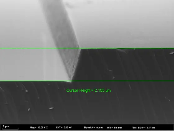
Wide-bandgap material processing
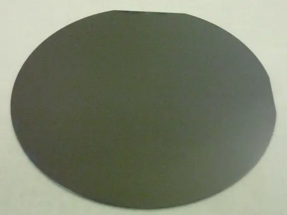
Four-inch SiO2 film deposition
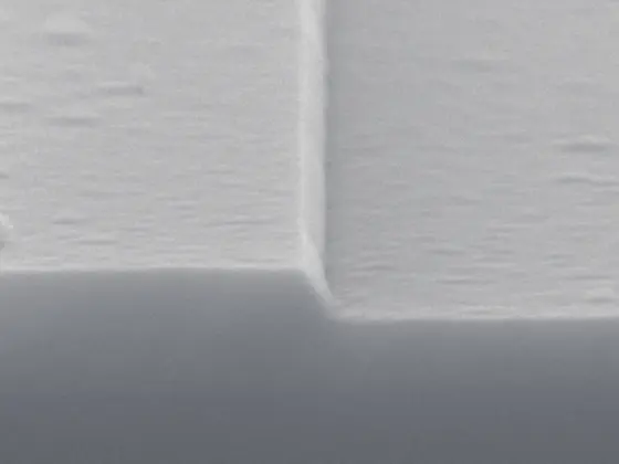
Silicon lens structure etch
Etching, deposition, and plasma treatment for device R&D and pilot-line process modules.
Process development for diamond, SiC, GaN, and other wide-bandgap material research.
TSV, wafer-level packaging, hybrid bonding, passivation, and thin-film stack workflows.
Deep silicon etch, release, and precision plasma process steps.
Equipment Platforms
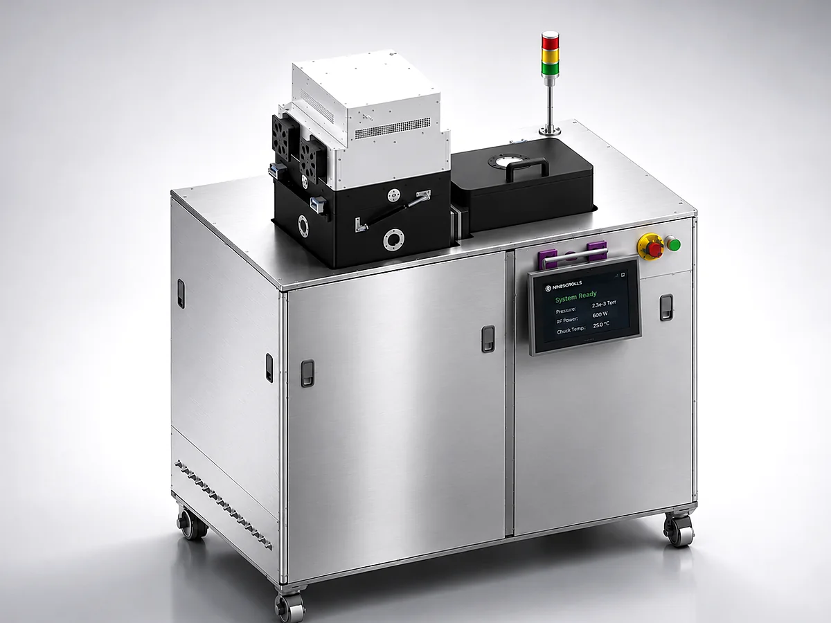
Platform
High-density plasma etching for demanding research processes.
Key Specifications
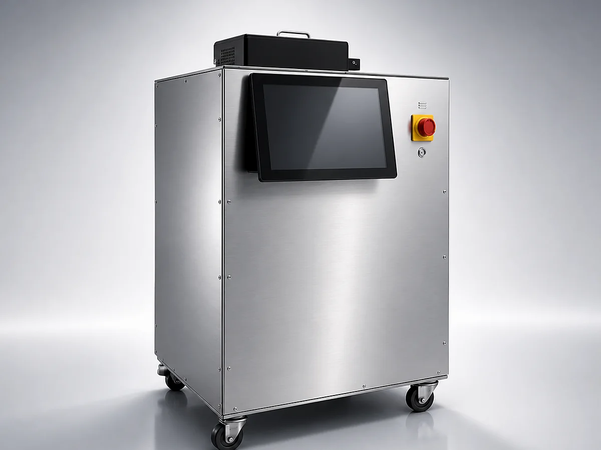
Platform
Reliable anisotropic etching for universities and R&D labs.
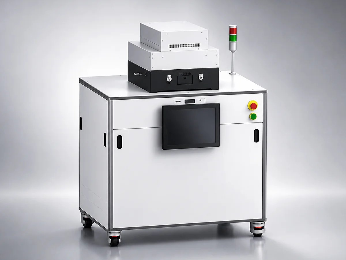
Platform
Plasma-enhanced thin-film deposition for research stacks.
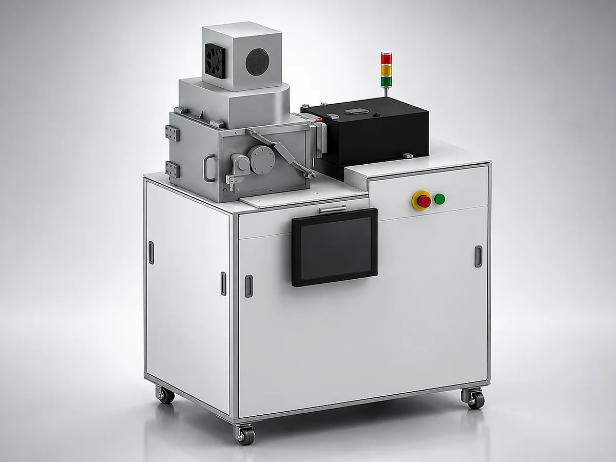
Platform
Conformal atomic-layer films for precise device structures.
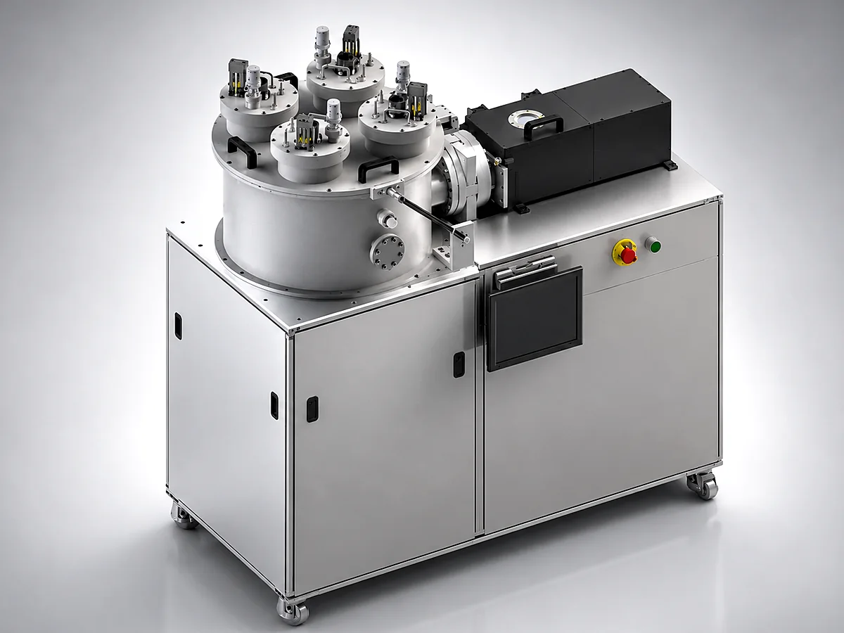
Platform
Physical vapor deposition for metals and functional films.
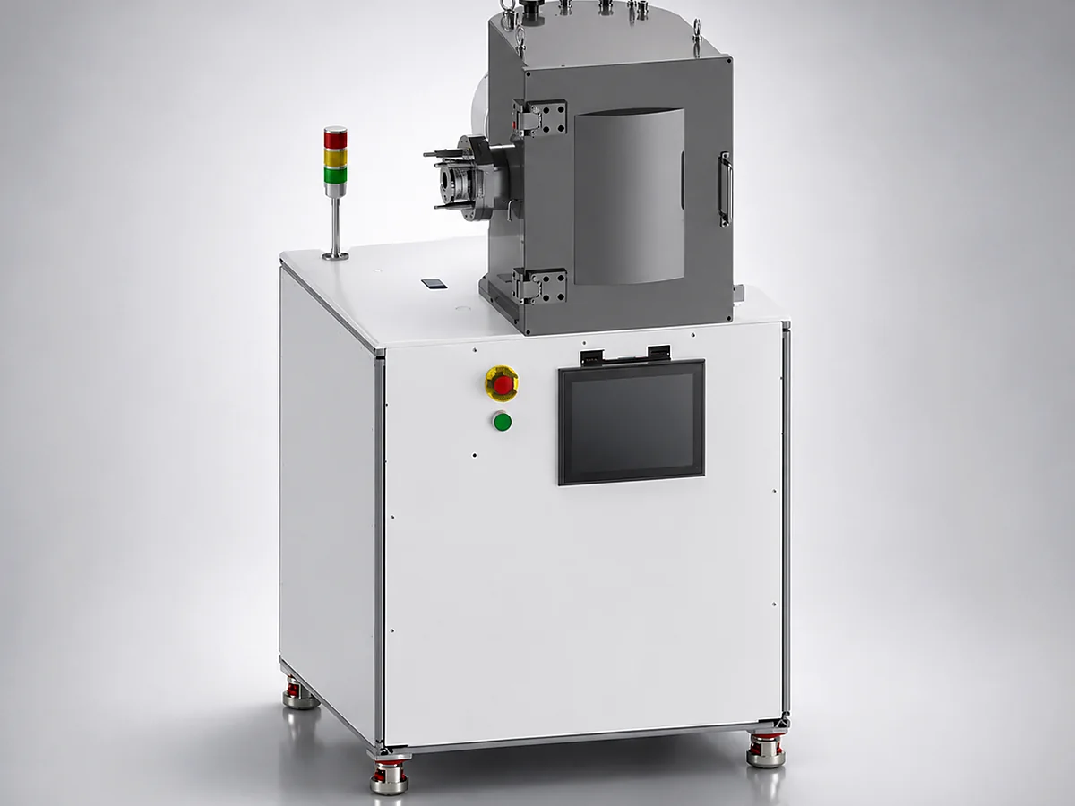
Platform
Directional ion beam processing for precise material removal.
Explore the complete equipment lineup
Compare additional platforms, including E-Beam Evaporation, HDP-CVD, Coater/Developer, stripping, and plasma cleaner systems.
Research evidence
Independent labs at universities and research institutes have used the plasma, deposition, and vacuum process platforms we represent in their published work.
92 verified studies across the platforms we represent · and growing
ICP etching
ICP-100A
PhotoniX
2022 · Research using the ICP etching platform we represent.
View source ↗RIE etching
RIE-150A
Light: Science & Applications
2026 · Research using the RIE etching platform we represent.
View source ↗Magnetron sputtering
Sputter-100
Energy & Environmental Science
2024 · Research using the magnetron sputtering platform we represent.
View source ↗RIE etching
RIE 100
Nature Communications
2021 · Research using the RIE etching platform we represent.
View source ↗Knowledge Center
Designed & Supported in the USA
Engineering-first Design
Two-Year Standard Warranty
Global Research Customers
Request a quote
Tell us your material stack, target process, and lab requirements. A NineScrolls engineer can help map the right platform and configuration.