Photoresist Stripping
Oxygen plasma chemistry removes PR and organic films through controlled ashing while reducing wet-strip chemical burden.
PR removalResist ashDescum
Equipment Platform
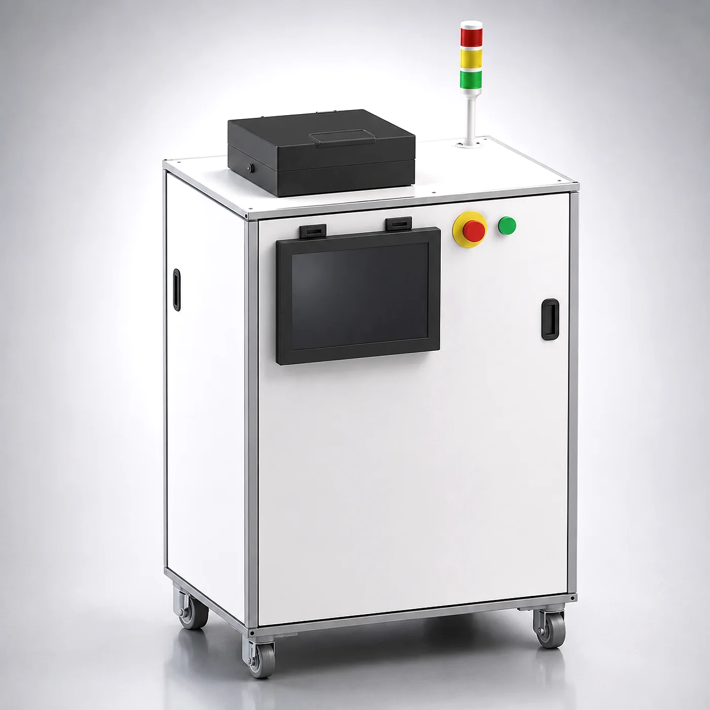
Dedicated plasma stripping and ashing for photoresist removal, post-etch residue cleaning, organic contamination removal, and damage-sensitive semiconductor process flows.
Wafer Size
4-12 in
RF Power
300-1000 W
Temperature
5 to 200 °C
Endpoint
Automated
Process-first configuration
Striper selection starts with resist thickness, hard-bake history, wafer size, temperature limit, endpoint strategy, residue type, target gas chemistry, and whether the process must protect low-k, Cu, III-V, MEMS, or 2D material stacks.
Oxygen plasma chemistry removes PR and organic films through controlled ashing while reducing wet-strip chemical burden.
Process windows can target polymer sidewall residue, organic contamination, and post-patterning clean-up after dry etch steps.
Temperature, ion exposure, and gas chemistry selection matter when cleaning low-k, Cu, III-V, MEMS, and 2D material stacks.
Core Process Windows
RF power and 5 to 200 °C wafer-stage control help engineers balance strip rate, residue removal, and thermal budget for resist and polymer workflows.
Automated endpoint detection and repeatable process recipes support cleaner handoff from lithography and etch into deposition, metrology, or bonding steps.
O2, O2/CF4, O2/N2, H2/N2, forming gas, and Ar/O2 decisions depend on resist condition, residue chemistry, and underlying material sensitivity.
Technical Specifications
Review core platform capabilities for initial process planning. Our engineering team will confirm the final gas manifold, vacuum, wafer handling, endpoint, and temperature options during quote review.
Applications
Photoresist stripping
Plasma ashing
Post-etch residue cleaning
Organic contamination removal
Surface activation and descum
2D material residue cleaning
Research evidence
Related Resources
Resource
O2 plasma chemistry, downstream vs direct plasma, gas selection, endpoint detection, and equipment selection
Resource
Barrel, downstream, and RIE-mode architectures, temperature effects, endpoint methods, and striper vs plasma cleaner decisions
Resource
Residue types, dry and wet cleaning methods, in-situ vs ex-situ tradeoffs, and damage-free cleaning strategies
FAQ
Choose a dedicated plasma striper when resist removal, ashing, post-etch residue cleaning, endpoint detection, wafer-scale uniformity, and controlled temperature are the core process requirements. A plasma cleaner is better for lower-power surface activation, bonding preparation, and general sample cleaning.
The Striper is positioned for organic materials including PR, PMMA, PS nanospheres, polymer residue, 2D material process residues, and organic contamination removal.
The Striper supports 4 inch to 12 inch wafers, 300 to 1000 W RF power, 5 to 200 °C temperature control, automated endpoint detection, and an approx. 0.8m x 0.8m compact footprint.
Request a quote
Share your resist type, wafer size, residue source, underlying materials, temperature limit, gas chemistry, endpoint needs, and timeline.