Space-Constrained Labs
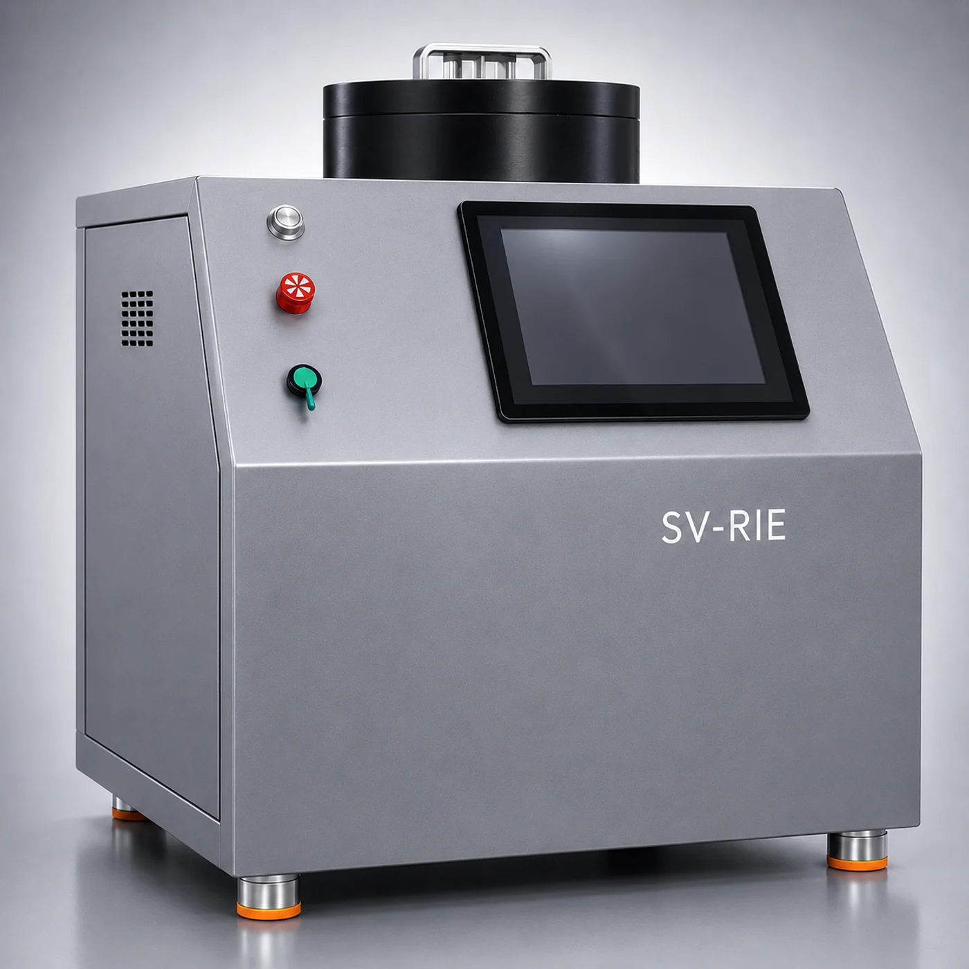
The SV-RIE format fits RIE capability into a compact footprint for universities, shared labs, and pilot-scale environments.
700 x 793 mmOne-piece designResearch lab fit
Equipment Platform
A space-efficient SV-RIE platform for labs that need true anisotropic plasma etching capability without the footprint of a full-size RIE system.
RF Power
300 or 500 W
Wafer Size
Up to 8 in
Footprint
700 x 793 mm
Best For
R&D / FA labs
Process-first configuration
Compact RIE selection starts with the materials you need to etch, target anisotropy, available lab footprint, RF power requirement, gas chemistry, and whether the workflow is routine resist removal, failure analysis, or rapid device prototyping.
The SV-RIE format fits RIE capability into a compact footprint for universities, shared labs, and pilot-scale environments.
Supports common PR, PMMA, organic polymer, and descum workflows where plasma cleaner capability is not enough.
Useful for package opening, passivation access, and rapid process development where labs need responsive in-house etch access.
Core Process Windows
The defining constraint is lab space: SV-RIE keeps true reactive ion etching capability available to teams that cannot allocate a full-size system footprint.
Model number sets maximum wafer size (4, 6, or 8 inches) and RF power is chosen separately at 300 W or 500 W, so labs pay for the sample size and process window they actually need.
The platform is positioned for photoresist, PMMA, HMDS, organic films, and Group IV and silicon-based process stacks in R&D settings.
Technical Specifications
Review series-level capabilities for initial process and model selection. Gas routing is configured per application within the 2-3-line system; our engineering team will confirm the manifold, pump, wafer handling, and model during quote review.
Applications
Space-constrained research labs
Failure analysis
Photoresist removal
Polymer descum
Passivation layer removal
Rapid device prototyping
Research evidence
Related Resources
Resource
RIE principles, process control, and equipment selection
Resource
How to choose RIE, ICP-RIE, DRIE, IBE, and compact etch platforms
Resource
Plasma mode comparison for process and equipment planning
FAQ
The Compact RIE (SV-RIE) is a one-piece platform that fits true reactive ion etching capability into a 700 x 793 mm footprint, so research and failure analysis groups can run RIE processes without allocating a full-size system bay.
The Compact RIE is specified for photoresist, PMMA, HMDS, organic films, and Group IV and silicon-based materials. Specific film stacks and the matching gas chemistry are confirmed with process engineering during quote review.
Model number tracks maximum wafer size: SHL100SV-RIE up to 4 inches, SHL150SV-RIE up to 6 inches, and SHL200SV-RIE up to 8 inches. RF power is a separate configuration choice of 0-300 W or 0-500 W at 13.56 MHz with automatic matching.
Request a quote
Share your target films, wafer size, process gases, RF power needs, available footprint, and timeline.