Deep Silicon Etching
High-density plasma process control for MEMS, TSV, Bosch-style workflows, and profile-sensitive silicon removal.
High aspect ratioSidewall controlMEMS and TSV
Equipment Platform
High-density plasma etching for silicon, MEMS, diamond, and compound semiconductor research.
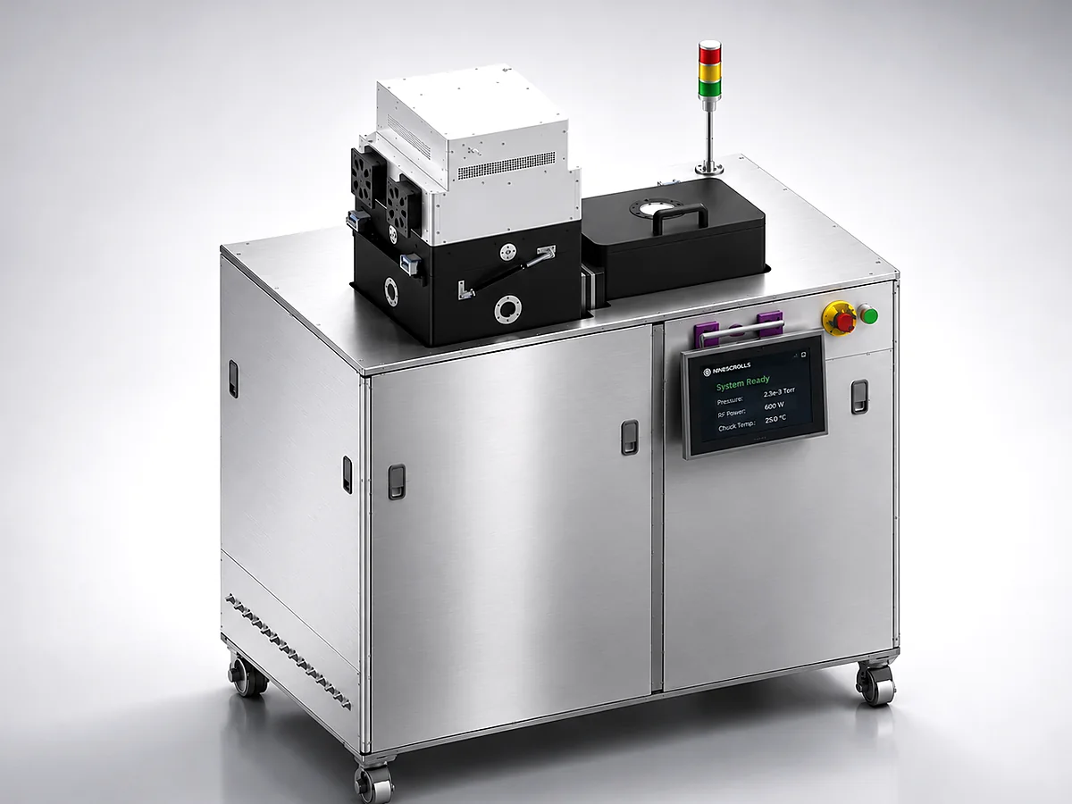
Configuration dependent. Final specifications confirmed during engineering review.
Budgetary range: US$189,000–$209,000. Budgetary reference based on two recent research-platform configurations. Final pricing depends on process chemistry, pumping, chuck cooling, automation, installation, and destination taxes or duties.
This platform is configured and quoted to your process — it is not sold online.
How it works
Follow ion-assisted surface reactions through a representative etch sequence.
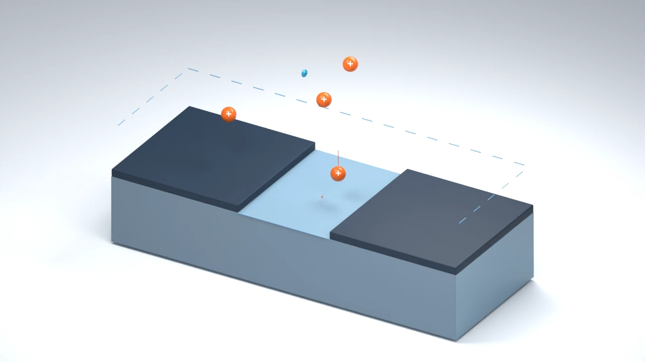
 Ions
Ions Reactive species
 Volatile products
Representative configuration with RF bias. Schematic — not to scale. Chemistry and results depend on the recipe.
Process-first configuration
ICP-RIE purchases usually start with materials, profile goals, wafer size, thermal control, gas chemistry, and allowable damage. These process requirements guide the final platform configuration.
High-density plasma process control for MEMS, TSV, Bosch-style workflows, and profile-sensitive silicon removal.
Independent source and bias control for GaN, GaAs, InP, SiC, Ga2O3, and related device research.
Configurable plasma chemistry and chuck temperature options for diamond, sapphire, and hard-to-process materials.
Core Process Windows
Separate RF generators let you tune plasma density and ion bombardment more independently, giving you more control over etch rate, selectivity, profile, and substrate damage.
Helium backside cooling improves heat transfer between the wafer and the temperature-controlled electrode, which helps hold wafer temperature steady during the etch. An optional -70 to 200 °C stage extends the range for low- and high-temperature chemistries.
A chamber liner and a configurable plasma discharge gap let the chamber be set up for the chemistry and materials it will run.
Technical Specifications
Review core platform capabilities for initial system selection. Final configurations are confirmed with our engineering team during quote review.
Applications
Silicon MEMS and TSV: deep, profile-controlled etching
Wide-bandgap power and RF: GaN, SiC, Ga₂O₃
III-V photonics: GaAs and InP
Diamond films: nucleation-layer removal
Optical microstructures: sapphire antireflection arrays, silicon microlenses
2D materials and refractory metals: MoS₂, BN, graphene, W, Ta, Mo
Failure analysis: SiO₂, SiNx and silicon layer removal
Process detail for each application area.
Research evidence
Published work using the ICP etching platform we represent · 20 papers
Sub-10-nm Lithography for Sn4-Oxo Clusters: Effect of Molecular Polarity on Sensitivity and Resolution
Advanced Functional Materials 2025
Enhanced Lithography Performance with Imino/Imido Benzenesulfonate Photoacid Generator-Bound Polymer Resists
Small 2025
Femtosecond laser fabrication of SiC microlens arrays as integrated light homogenizer and splitter
IEEE Photonics Technology Letters 2023
Biomimetic sapphire windows enabled by inside-out femtosecond laser deep-scribing
PhotoniX 2022
Single Cubic Metalens for Compact 3D Microscopic Imaging with Extended Depth of Field
ACS Photonics 2026
Broadband Complex Amplitude-Modulated Metasurfaces for Nanoprinting and Vectorial Hologram with Continuously Varying Linear Polarization Distributions
Advanced Optical Materials 2024
High-Performance Color Printing and Information Encryption Enabled by Silicon Carbide Metasurface
Advanced Functional Materials 2026
Periodic Microstructures Fabricated by Laser Interference with Subsequent Etching
Nanomaterials 2020
Non-invasive and fully two-dimensional quantitative visualization of transparent flow fields enabled by photonic spin
Light: Science & Applications 2025
Diffraction-Free Omnidirectional Antireflection Binary Metasurface via Femtosecond Laser Hybrid Etching
Advanced Materials 2026
Mitigating the Thermal Bottleneck in Polycrystalline Diamond Films by Gradient ICP Etching of the Nucleation Layer
Materials 2026
Experimental study of inductively coupled plasma etching of patterned single crystal diamonds
Scientific Reports 2025
Integration of multifocal microlens array on silicon microcantilever via femtosecond-laser-assisted etching technology
Micromachines 2022
Selenization Mechanism of Nearly 4 in. Single-Oriented PtSe2 and PtSe2/n-Si/n+-Si 2D-3D PIN Wide-Spectrum Polarization Detectors
ACS Applied Materials & Interfaces 2025
Neural-Optic Co-Designed Polarization-Multiplexed Metalens for Compact Computational Spectral Imaging
Laser & Photonics Reviews 2024
Sapphire concave microlens arrays for high-fluence pulsed laser homogenization
IEEE Photonics Technology Letters 2019
Broadband and high-speed micro-scale PtSe2/Si 2D-3D PIN photodetector for on-chip polarization-encoded communication and imaging
Applied Surface Science 2026
Rapid engraving of artificial compound eyes from curved sapphire substrate
Advanced Functional Materials 2019
Silicon three-dimensional structures fabricated by femtosecond laser modification with dry etching
Applied Optics 2017
Wear-resistant blazed gratings fabricated by etching-assisted femtosecond laser lithography
Journal of Lightwave Technology 2021
Process evidence
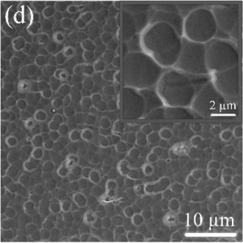
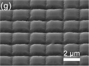
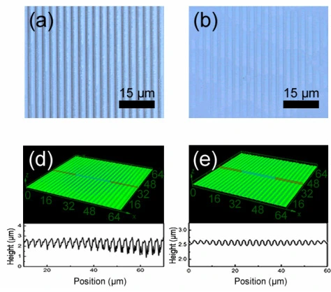
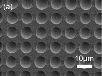
Peer-reviewed results published by research groups working on this ICP-RIE platform family — diamond, sapphire, GaAs, and silicon. Each card names the system its paper used and links to the source.
System Views
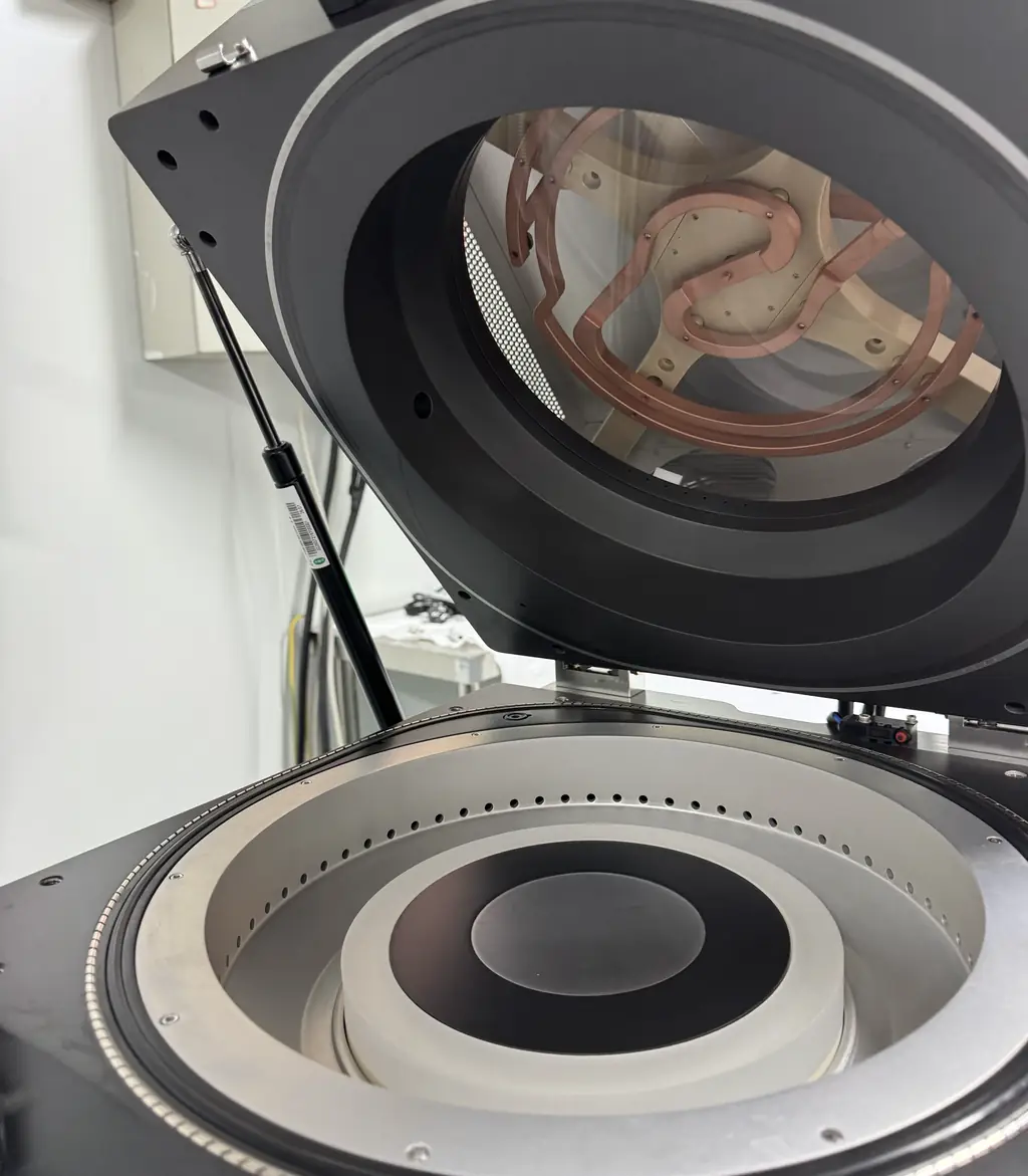
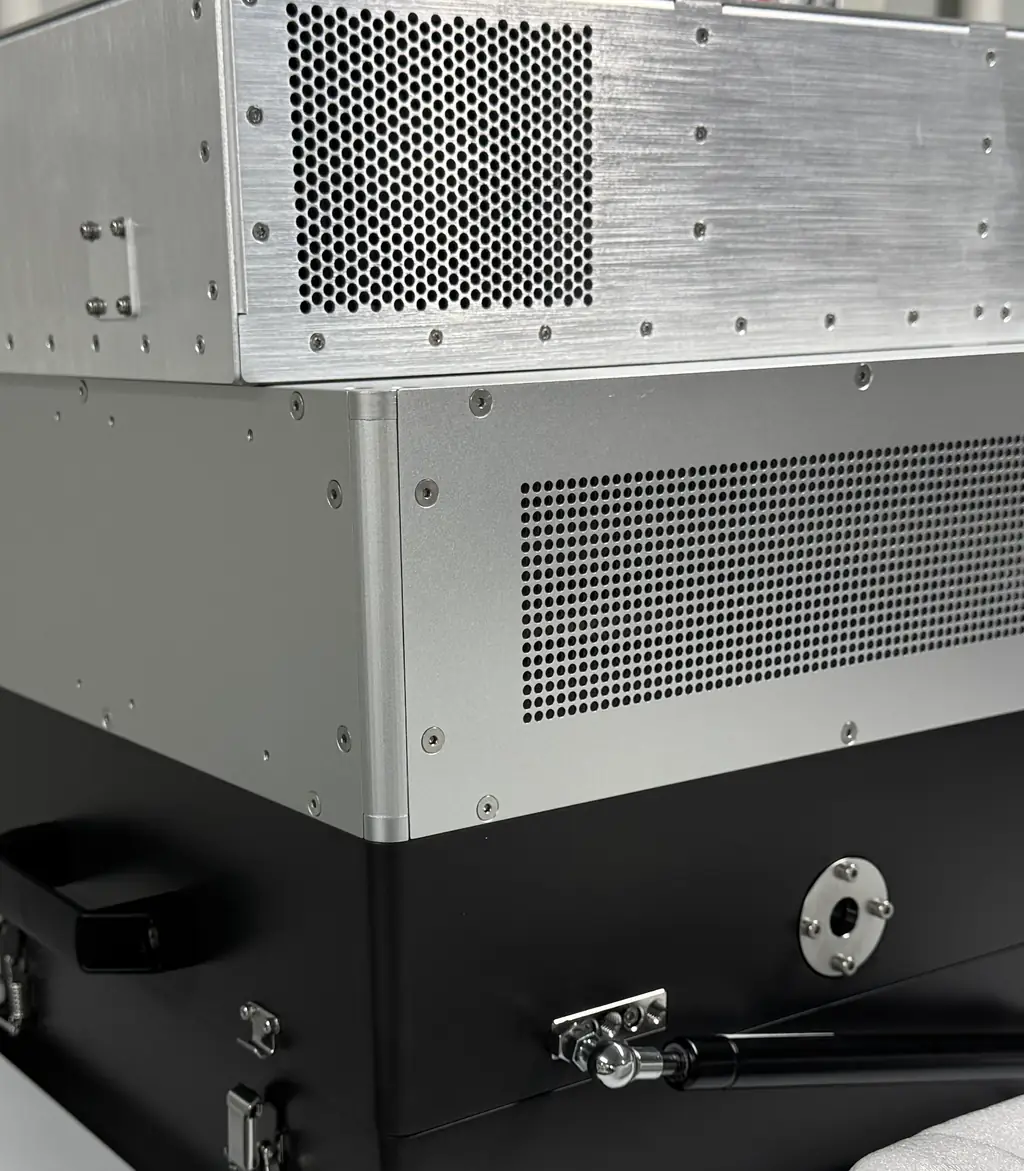
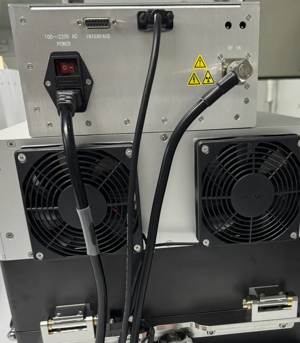
Actual system photos: the chamber with the lid raised, the etch module exterior with the RF unit on top, and the module rear with its power, interface, and RF-in connections. Use them to review the source geometry and service access before configuration review.
System overview · 2 minutes
See how independent ICP source and RF bias control shape the etch, follow the gas, vacuum and thermal paths through the system, and explore the chamber architecture and optional load-lock.
Representative configuration; options vary. Process results, transfer mechanics and selected internal views are illustrative. Software screens show example values. The load-lock is optional.
Service & Support
Every ICP-RIE system is factory-acceptance tested before shipment, with the acceptance and as-shipped configuration documented. NineScrolls supports the system through commissioning and operation, for both equipment issues and process questions.
Service terms and support optionsDelivered with every system
Standard coverage
Before shipment, the system is tested for vacuum, RF, gas control and etch performance on standard silicon test wafers, using an agreed FAT protocol or the NineScrolls standard FAT procedure. Customer-specific materials and process results are outside the standard FAT scope.
Remote commissioning guidance is included. On-site installation, commissioning and initial process verification can be quoted with the system, using verification conditions agreed in advance.
Operator training can be quoted with the system. Every supported system also receives machine-specific documentation and training materials through NineScrolls Academy.
Diagnosis starts remotely, from alarm records, recipe data and photos. On-site service can be arranged when needed; labor and travel are quoted unless covered by a service agreement.
Warranty replacement parts are supplied by NineScrolls. A recommended spare-parts package can be quoted based on the system configuration and support needs, and we can identify customer-held spares for critical components where warranted.
Related Resources
Resource
Technology guide for ICP-RIE principles
Resource
Process selection comparison
Resource
DRIE and deep silicon etch primer
Resource
Wide-bandgap diamond etch guide
FAQ
The ICP-RIE platform is designed for high-aspect-ratio silicon etching, MEMS fabrication, compound semiconductor processing, diamond processing, photonics, advanced packaging, and process development where independent plasma density and ion energy control matter.
ICP-RIE uses a high-density inductively coupled plasma source with separate bias control, allowing plasma density and ion energy to be tuned independently. Standard RIE is simpler and useful for many general etch workflows, but ICP-RIE provides a wider process window for demanding research applications.
The ICP-RIE platform supports 4 inch to 12 inch wafers, with configurable loading, gas, RF, and temperature options depending on process needs.
Use this product page when you are selecting an ICP-RIE etching system, checking wafer size, ICP power, bias control, gas lines, temperature range, applications, or quote requirements. Use the ICP-RIE Technology guide when you want to learn the principles of inductively coupled plasma generation, source power, bias power, and high-density plasma etching.
Request a quote
Share your material stack, target profile, wafer size, gases, temperature needs, and lab timeline.