
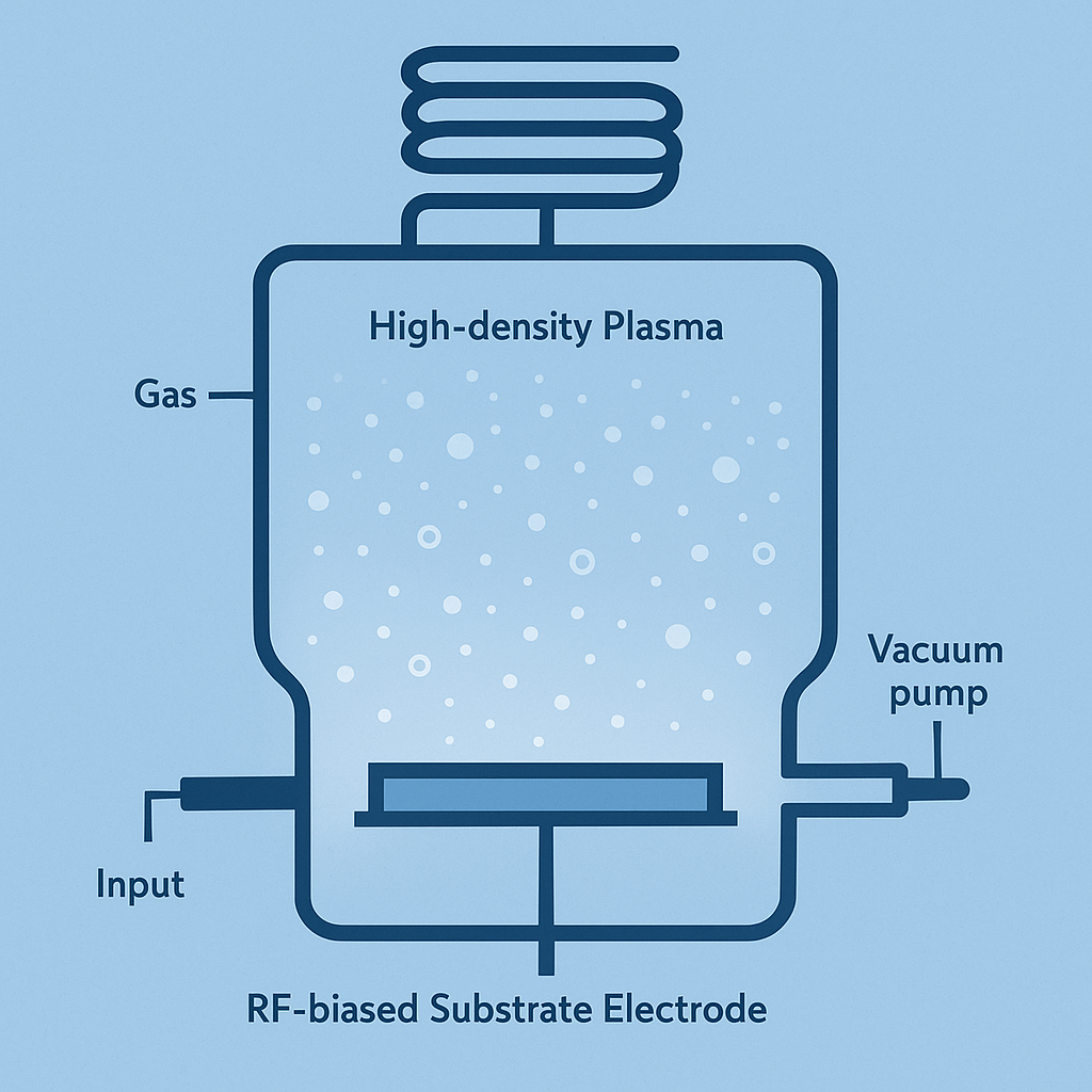
ICP-RIE (Inductively Coupled Plasma Reactive Ion Etching) is a high-density dry-etching technology that uses a radio-frequency induction coil to generate a dense plasma while a separate radio-frequency bias drives reactive ions into the wafer with controlled energy. An ICP etcher decouples plasma generation from ion acceleration, giving process engineers independent control over reactive-species density and ion bombardment energy. This separation is what distinguishes ICP plasma etching from conventional Reactive Ion Etching (RIE), where a single power supply sets both quantities at once. The result is faster, more anisotropic, and better-controlled etching across silicon, dielectrics, compound semiconductors, and metals.
TL;DR
ICP-RIE (inductively coupled plasma reactive ion etching) is a high-density dry etch that uses two independent radio-frequency supplies — a source coil that sets plasma density and a substrate bias that sets ion energy. Decoupling those two variables lets engineers tune etch rate, profile, selectivity, and substrate damage as separate dials rather than one compromise, which is what makes deep high-aspect-ratio silicon, hard wide-bandgap materials such as SiC and GaN, and volatility-sensitive III-V compounds practical to etch. This guide covers the underlying physics, the process trade-offs and failure modes, and the inflection points where a lab should move up from conventional RIE.
1) What Is ICP-RIE?
ICP-RIE is a two-source plasma etching process. A first radio-frequency supply drives an inductive coil that creates a high-density plasma, and a second radio-frequency supply biases the substrate electrode to accelerate ions toward the wafer surface. The combination delivers the chemical reactivity of a dense plasma with the directional ion bombardment needed for vertical, anisotropic profiles.
In a conventional RIE system, a single capacitively coupled radio-frequency electrode both generates the plasma and accelerates the ions. Raising the power to increase plasma density therefore also raises ion energy, and lowering ion energy to protect a sensitive surface simultaneously starves the plasma of reactive species. Because the two effects are linked, the operating window is narrow.
An ICP etcher breaks that coupling. The inductive source controls how many reactive radicals and ions are produced, while the bias supply independently sets how hard those ions strike the wafer. This is the defining characteristic of ICP plasma etching and the reason it has become the standard high-density plasma etching platform for demanding semiconductor, photonic, and MEMS device fabrication. Engineers can run a dense plasma at low ion energy for gentle, selective etching, or a dense plasma at high ion energy for deep, directional features, without sacrificing throughput.
2) How ICP Plasma Is Generated
The plasma in an ICP-RIE chamber is produced inductively rather than capacitively. A radio-frequency current, typically at 13.56 MHz, flows through a coil wound around or above a dielectric window at the top of the chamber. That oscillating current generates a time-varying magnetic field inside the chamber, and by Faraday's law the changing magnetic field induces an azimuthal electric field in the gas below the window.
Free electrons in the gas are accelerated by this induced electric field. Because the field oscillates with the coil current, electrons are continuously heated as they oscillate in this induced electric field, gaining enough energy to ionize neutral gas molecules through collisions. Each ionizing collision releases additional electrons, which are themselves heated and go on to ionize further molecules. This sustained, efficient electron heating produces a dense, well-ionized discharge.
Because the power is transferred through a magnetic field rather than directly across a sheath, the coil can pump large amounts of energy into the electron population without imposing a correspondingly large voltage on the wafer. That is precisely what enables high-density plasma etching: the inductive source maintains a copious supply of reactive radicals and ions, while the wafer-side conditions remain free to be tuned separately. The dielectric window isolates the coil electrically from the plasma so that power couples inductively into the gas rather than capacitively into the electrode, which is the physical basis of the density-versus-energy decoupling that defines ICP-RIE.
3) ICP Source Power vs RF Bias Power
The single most important concept in ICP-RIE is the separation of two power supplies that perform two different jobs. ICP source power, applied to the induction coil, governs plasma density: how many ions and reactive radicals are created per unit volume. RF bias power, applied to the substrate platen electrode, governs ion energy: how forcefully those ions are accelerated across the sheath and into the wafer.
The bias supply works by establishing a DC self-bias on the wafer-bearing electrode. Because electrons are far more mobile than ions, the radio-frequency-driven electrode charges negatively relative to the plasma, and the resulting sheath voltage accelerates positive ions toward the surface. Raising the bias power deepens the DC self-bias and increases the average ion energy striking the wafer, which sharpens directionality and physical sputtering. Lowering it softens the bombardment to reduce damage and improve selectivity.
Crucially, these two controls are largely independent: increasing ICP source power raises ion flux and etch rate with only a modest effect on ion energy, while increasing bias power raises ion energy with little effect on the bulk plasma density. This independent ion density control is the key advantage over capacitively coupled plasma (CCP) reactors and standard RIE, where one knob sets both. In a CCP or RIE tool, achieving a high etch rate forces high ion energy, which can sputter the mask, damage the substrate, or degrade selectivity. How that independence translates into real process outcomes — with etch rate, profile, selectivity, and substrate damage as separately tunable variables rather than a single compromised operating point — is the subject of the next section.
4) Decoupled Control in Practice
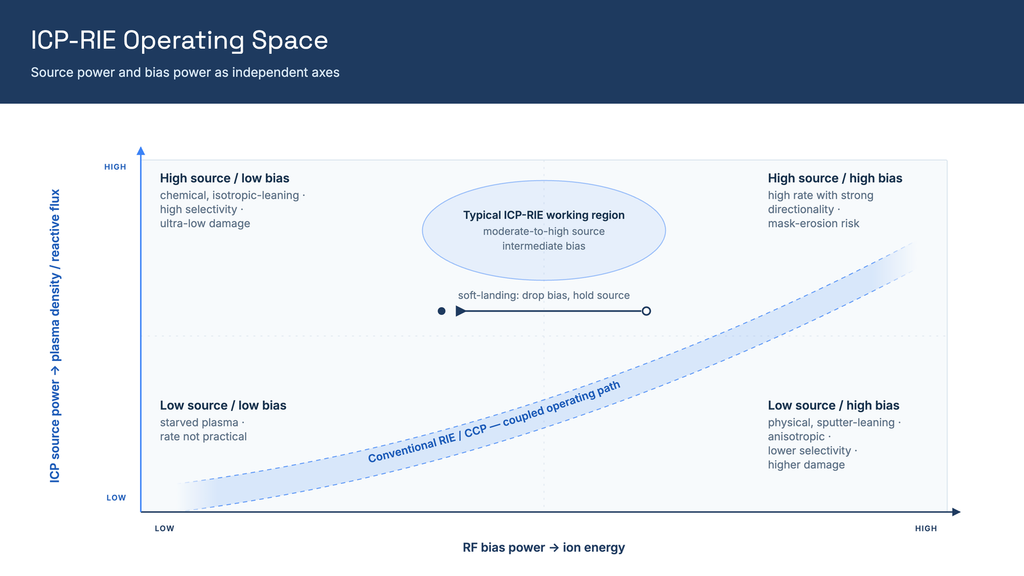
The practical value of ICP-RIE is easiest to see if you treat source power and bias power as two orthogonal axes. Source power is the "how much reactive flux" axis; bias power is the "how hard the ions land" axis. Because the two move almost independently, a recipe is a point in a two-dimensional space rather than a position on a single line. The two extreme corners of that space bracket the range of behavior an ICP etcher can access.
| Operating regime | Radical / ion density | Ion energy | Etch character | Selectivity to mask & underlayer | Lattice / mask damage |
|---|---|---|---|---|---|
| High source / low bias | High | Low | Chemical, isotropic-leaning | High | Ultra-low |
| Low source / high bias | Low | High (directional) | Physical, anisotropic / sputter-leaning | Lower | Higher |
In the high-source / low-bias corner, the dense plasma supplies an abundance of reactive radicals while the ions arrive softly. Material removal is driven by chemistry, so it leans isotropic, spares the mask and underlying layers, and inflicts minimal lattice damage. This is the regime for gentle, selective, damage-sensitive work — clearing a film over a thin gate dielectric, or stopping cleanly on a delicate underlayer without driving ions into it.
In the opposite low-source / high-bias corner, the plasma is sparse but the ions are energetic and strongly directional. Removal is dominated by physical sputtering: the profile becomes highly anisotropic and vertical, but the etch is far less chemically selective — the mask erodes along with the target — and the energetic bombardment raises substrate damage. This is the regime for cases where directionality matters more than selectivity.
Real recipes almost never sit at a corner. Most useful etches combine a moderate-to-high source power for rate with an intermediate bias that supplies just enough directionality for vertical sidewalls without over-sputtering the mask. Because the two axes are independent, an engineer can slide along either one deliberately — for example, dialing bias down in the final seconds of an etch to soft-land on a sensitive stop layer while keeping source power high to preserve throughput. Etch rate, profile, selectivity, and damage stop being a single fixed trade-off and become four dials that can be set against one another on purpose.
This is exactly what a conventional RIE or CCP reactor cannot do. With a single supply setting both density and energy, its operating point is confined to one diagonal line through the space above: pushing the etch rate up drags ion energy — and damage — up with it, and backing the energy off starves the plasma of reactive species. ICP's second, independent supply is what turns that line into a plane, and the freedom to choose any point in the plane is the platform's defining process advantage.
5) Why ICP Achieves High Plasma Density
The efficiency of inductive power transfer is what gives ICP-RIE its characteristically high plasma density. Inductive coupling deposits energy directly into the electron population across the volume of the discharge, sustaining far more ionization than the sheath-limited capacitive coupling of a conventional RIE electrode. As a result, ICP sources routinely reach ion densities on the order of 1011–1012 cm-3, roughly one to two orders of magnitude higher than the 109–1010 cm-3 typical of capacitively coupled or conventional RIE plasmas.
This high density translates directly into a large flux of reactive radicals and ions at the wafer, which is the origin of the high etch rates ICP-RIE is known for. Equally important, the dense plasma can be sustained at low pressure, often just a few millitorr. Low pressure lengthens the mean free path of ions traveling through the sheath, so ions reach the wafer with fewer collisions and a more tightly collimated, near-vertical trajectory. Directional ions arriving with minimal angular spread are what produce anisotropic, high-aspect-ratio profiles with straight sidewalls. The combination of high density for rate and low pressure for directionality is the technical foundation of the platform's anisotropy advantage.
6) High-Aspect-Ratio & Deep Etching
High-aspect-ratio and deep etching is where the density and low-pressure advantages of the previous section combine into a capability. Etching a feature whose depth greatly exceeds its width — a through-silicon via, a deep MEMS trench, a 3D memory channel — is limited by two things at once: whether enough reactive species can reach the bottom of a narrow, deepening hole, and whether the ions doing the work arrive vertically enough to keep etching the floor rather than the walls. The dense ICP plasma addresses the first by supplying a large reactive flux that keeps the reaction fed deep into the feature, and the low operating pressure addresses the second by keeping ions collimated and near-vertical so they travel to the trench floor with little angular spread.
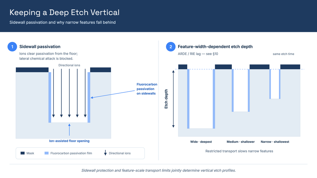
Directional ions alone, however, do not guarantee vertical walls — chemistry attacks sideways as readily as downward. The missing ingredient is sidewall passivation: a thin protective film is formed on the feature walls while the vertical ion flux continuously clears it from the floor. Etching therefore proceeds downward while lateral attack is suppressed, producing straight, deep sidewalls. This one principle underlies both continuous mixed-chemistry high-aspect-ratio etches and the time-multiplexed schemes used for the deepest silicon structures.
The dominant time-multiplexed scheme alternates discrete etch and passivation steps to reach very high aspect ratios in silicon; we cover its mechanics, scallop control, and process trade-offs in our deep reactive ion etching (Bosch process) guide. A lower-temperature alternative suppresses sidewall attack by condensing passivation continuously rather than cycling it, with its own profile and throughput characteristics — compared side by side in our cryogenic etching vs. Bosch process article. Both rely on the same ICP-RIE foundation of high density for rate and independent bias for directionality.
Deep etching also exposes the platform's characteristic limit: as features grow deeper and narrower, their etch rate falls behind wider ones because reactants struggle to reach — and by-products struggle to leave — the bottom of a high-aspect-ratio trench. This aspect-ratio-dependent etching (ARDE), or RIE-lag, together with its uniformity and profile counterparts, is the main practical constraint on deep processes; the failure modes and how to manage them are treated in the profile, damage, and uniformity section below.
7) ICP-RIE Equipment Architecture
An ICP-RIE system is built around its two plasma sources, with supporting subsystems that make the process repeatable and well controlled. Understanding the architecture clarifies where the capability comes from rather than serving as a buying guide.
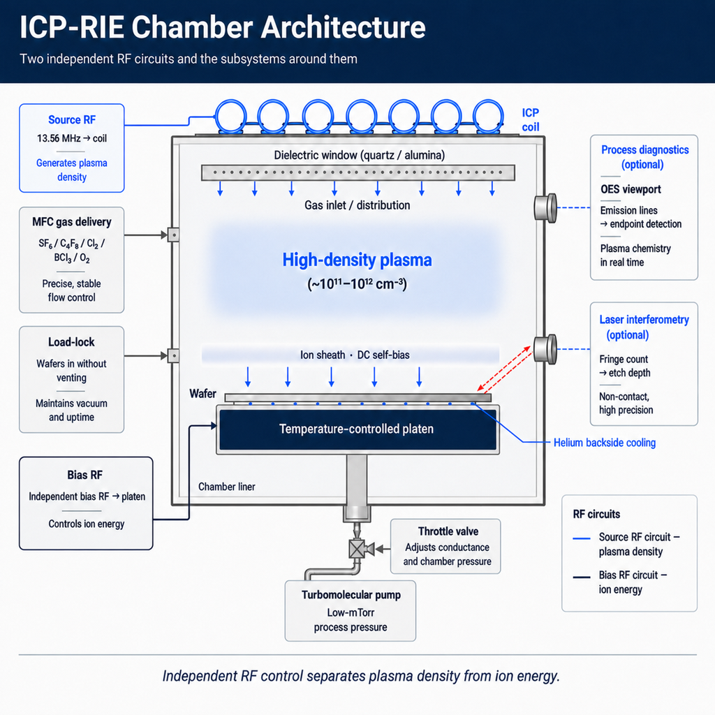
- Induction coil and dielectric window: A radio-frequency coil sits outside a dielectric (typically quartz or alumina) window at the top of the chamber. The window passes the magnetic field while keeping the coil electrically isolated from the plasma, ensuring inductive rather than capacitive coupling.
- Process chamber: The reaction volume where gas is ionized and etching occurs, held under vacuum and lined with materials chosen for chemical compatibility with aggressive halogen chemistries.
- Biased substrate electrode: The wafer rests on a platen connected to the independent radio-frequency bias supply. This electrode is usually temperature-controlled, frequently with helium backside cooling, to hold the wafer at a setpoint during high-power etching or to enable cryogenic processes.
- Gas delivery: Mass flow controllers (MFCs) meter precise quantities of process gases such as SF6, C4F8, Cl2, BCl3, or O2 into the chamber so that chemistry can be tuned and reproduced.
- Pressure control: A turbomolecular pump and a throttle or capacitance-manometer-controlled valve hold chamber pressure at the low-millitorr setpoint required for long mean free path and anisotropy.
- Endpoint detection: Optical emission spectroscopy (OES) tracks plasma emission lines to detect when a layer clears, while laser interferometry monitors etch depth in real time, both improving process control and repeatability.
- Load-lock: A vacuum transfer chamber lets wafers enter and exit without venting the process chamber, preserving chamber conditioning and improving throughput and cleanliness.
8) Semiconductor Manufacturing Applications
Because ICP-RIE delivers high etch rates, strong anisotropy, and independent control of density and ion energy, it is applied across logic, memory, power, photonic, and packaging fabrication. The following examples illustrate where the platform's capabilities matter most.
Logic & Memory
In advanced CMOS logic and memory, ICP-RIE etches gate stacks, shallow-trench isolation, contact and via openings, and the deep, high-aspect-ratio features of 3D NAND. The ability to run a dense plasma at controlled, relatively low ion energy is essential here: it protects thin gate dielectrics and ultra-shallow junctions from ion-induced damage while still clearing material at production throughput. Tight profile control over millions of identical features also keeps critical dimensions within the narrow tolerances that modern nodes demand.
SiC & GaN Power Devices
Wide-bandgap power devices are a major ICP-RIE application. Gallium nitride is etched for mesa isolation, gate recess, and ohmic-contact formation, and silicon carbide for trench, gate, and edge-termination structures in high-voltage devices. Why these hard, inert materials specifically require an ICP source rather than a conventional RIE tool is taken up in the materials section that follows; the point here is the breadth of power-device features the platform patterns.
III-V Photonics
Indium phosphide, gallium arsenide, and related III-V compounds are patterned to build laser ridges, waveguides, photonic crystals, gratings, and modulators, all of which need extremely smooth, vertical sidewalls to minimize optical scattering loss. The etch physics that delivers those sidewalls on these volatility-sensitive materials is detailed in the materials section below.
Advanced Packaging (TSV & Deep Silicon)
In 3D integration and advanced packaging, ICP-RIE forms through-silicon vias (TSVs) and other deep silicon structures, and the same deep-silicon capability serves MEMS sensors, actuators, and microfluidic channels. The high-aspect-ratio mechanism these features rely on is covered in the high-aspect-ratio section above.
9) Material-Specific ICP-RIE Behavior: Where Standard RIE Hits Its Limits
The clearest way to understand why ICP-RIE exists is to look at the materials a conventional single-supply RIE tool struggles to etch well. In each case the difficulty traces back to the same root: the etch demands more reactive flux, or a different balance of chemistry and energy, than a coupled reactor can deliver without pushing ion energy to destructive levels. Decoupling density from energy is what makes these materials tractable.
SiC, GaN, and Wide-Bandgap Materials
Silicon carbide and gallium nitride owe their value as power-device materials to strong, high-binding-energy bonds — and that same bond strength is what makes them chemically inert and slow to etch. Breaking those bonds at a useful rate requires a large flux of energetic ions and reactive radicals at the surface. In a conventional RIE tool the only way to raise that flux is to raise power, which simultaneously raises ion energy — and the elevated bias erodes the etch mask and drives lattice damage deep into a device layer that must stay electrically pristine. An ICP source resolves the conflict by generating the high ion and radical flux from the coil independently, so the material is removed at a practical rate while the bias, and therefore the ion energy and the damage it causes, is held only as high as the profile requires. Fluorine chemistries are typical for SiC and chlorine chemistries for GaN, but the platform-level point is the same: it is the independent high flux of the ICP source, not brute-force bias, that makes wide-bandgap etching practical.
III-V Compounds (InP, GaAs)
Indium phosphide, gallium arsenide, and related III-V compounds present a different problem: volatility balance. Etching a compound cleanly requires that all of its constituent elements leave the surface as volatile by-products at comparable rates. In the indium compounds the indium-bearing by-products are considerably less volatile than the phosphorus- or arsenic-bearing ones, and their volatility is strongly temperature-dependent: run the surface too cool and involatile indium species accumulate and roughen it, too hot and the group-V element is lost preferentially. ICP-RIE supplies the two controls needed to manage this — a high-density plasma to keep every species reacting and desorbing, and, because bias and source are separate, the freedom to hold ion energy low enough to avoid roughening while a temperature-controlled platen keeps the surface in the window where indium by-products stay volatile. The result is the smooth, vertical sidewalls photonic devices demand. The metal and hard-mask layers that accompany these stacks carry their own etch chemistry, covered in our metal etching complete guide.
10) Profile, Damage & Uniformity Control
The same high plasma density that makes ICP-RIE fast also amplifies a family of profile and uniformity problems. Because the platform is so often used for deep, high-aspect-ratio features, these effects show up more strongly here than in shallow conventional RIE, and managing them is a large part of ICP process development.
ARDE / RIE-Lag
Aspect-ratio-dependent etching, introduced earlier, is the tendency for narrow, deep features to etch more slowly than wide, shallow ones on the same wafer. As a trench deepens, reactant transport to the floor and by-product removal from it both become rate-limiting, so the local etch slows in exactly the features that need to go deepest. A closely related transport effect, microloading, makes the local etch rate depend on the surrounding pattern density, so densely packed and isolated features can clear at different rates across the same wafer. A layout with mixed feature sizes and pattern densities therefore reaches target depth at different times, and the process must be tuned — through pressure, the passivation balance, and sometimes pulsing — so the slowest feature clears without over-etching the fastest.
Micro-Trenching, Notching, and Charging
High-density plasmas drive charging and ion-deflection effects. Micro-trenching — the narrow grooves cut into the floor right at the base of the sidewalls — comes chiefly from ions that reflect off the sloped sidewalls and converge their flux onto the trench-bottom corners; charge accumulating unevenly on the sidewalls adds to it by deflecting incoming ions off their vertical paths. That same sidewall charging is the primary driver of notching, where deflected ions pile up at the interface with an underlying dielectric and undercut the foot of the feature. Sidewall bowing arises when off-axis ions widen the mid-feature profile. These are ion-trajectory problems rather than chemistry problems, and they are managed by lowering ion energy where the profile allows, adjusting pressure, and increasingly by using pulsed plasma or pulsed bias to let accumulated charge dissipate between pulses.
Wafer Temperature and Helium Backside Cooling
The bridge from these problems to hardware is temperature. The dense ICP plasma deposits a large heat load on the wafer, and both etch chemistry and sidewall passivation are temperature-sensitive — a passivation film that holds a profile at one temperature can fail a few tens of degrees away, and the volatility-limited III-V materials above demand a tightly held setpoint. A simple parallel-plate RIE tool, running lower density and less demanding processes, can often tolerate a loosely controlled wafer temperature. An ICP tool generally cannot: it relies on helium backside cooling — a controlled flow of helium between the wafer and a temperature-regulated platen — to carry heat away efficiently and hold the surface at setpoint through a high-power etch. Precise, actively controlled wafer temperature is therefore not a luxury in ICP-RIE but a prerequisite for repeatable profiles and uniformity.
11) Endpoint Detection & Metrology
Knowing precisely when an etch has reached its target — a cleared layer or a set depth — matters especially in ICP-RIE, where the high etch rate leaves little margin between a completed etch and an over-etched one. Two in-situ techniques, both part of the equipment architecture described above, dominate.
Optical emission spectroscopy (OES) watches the light the plasma emits. Each reactive species and etch by-product radiates at characteristic wavelengths, so as a film clears and the by-product it was producing disappears — or as a newly exposed underlayer begins to contribute its own emission — the intensity of a chosen spectral line steps up or down, giving a real-time endpoint signal. The high density of an ICP plasma helps here: strong emission yields a clean, high-signal trace. The corresponding difficulty is that when the exposed area is very small the by-product signal can be faint against the bright bulk plasma, so careful line selection matters more as open area shrinks.
Laser interferometry measures depth rather than composition. A laser reflected from the etch front and the surface beneath it produces interference fringes that cycle as the etched depth changes, so counting fringes tracks depth in real time — indispensable for blind features such as partial-depth trenches and for the deep structures where a purely timed etch would drift. In practice the two are complementary: OES to detect a layer clearing, interferometry to hit a depth target.
12) Troubleshooting: ICP-RIE-Specific Failure Modes
Most ICP-RIE profile and uniformity defects trace back to the mechanisms in the two sections above. The table below maps common symptoms to their likely cause and the qualitative direction of the fix; specific setpoints always depend on the material, chemistry, and tool.
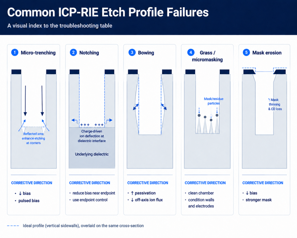
| Symptom | Likely cause | Qualitative corrective direction |
|---|---|---|
| Deep, narrow features lag shallow ones (uneven depth across the wafer) | ARDE / RIE-lag — transport-limited at the trench floor | Lower pressure to lengthen the mean free path; rebalance passivation; consider pulsed plasma; size the over-etch to the slowest feature within the mask budget |
| Narrow grooves at the foot of the sidewalls | Micro-trenching — ions reflected off the sidewalls (plus charge-deflected ions) converging at the trench-bottom corners | Reduce ion energy (bias); raise pressure slightly; pulse the bias to let charge dissipate |
| Lateral notch where the etch reaches an underlayer | Charging-driven notching at a dielectric interface | Reduce bias near endpoint; use pulsed plasma; minimize over-etch with better endpoint detection |
| Bowed (barrel-shaped) sidewalls | Off-axis ions widening the mid-profile; insufficient sidewall passivation | Increase passivation; lower pressure for better collimation; trim bias |
| Rough floor, "grass," or black silicon | Micromasking — residue or redeposited material shielding spots on the floor | Remove the micromask source (clean/condition the chamber, adjust the oxidant/passivant balance); briefly raise bias to clear residue |
| Mask eroding, poor selectivity | Ion energy too high for the mask material | Lower bias and lean on source-driven chemical etching; move to a more selective or thicker mask |
| Center-to-edge non-uniformity | Thermal or reactant-flux non-uniformity across the wafer | Improve wafer temperature control (helium backside cooling); check gas distribution and coil/match tuning |
| Profile or rate drifts run-to-run | Chamber-wall conditioning changing over time | Add a seasoning/clean cycle; monitor with OES; standardize idle and queue times |
13) Advantages of ICP-RIE
- High etch rate: The dense plasma supplies a large flux of reactive species, enabling fast material removal and strong throughput.
- High density at low pressure: Inductive coupling sustains high ionization at a few millitorr, combining ample reactivity with the long mean free path needed for directional etching.
- Independent energy and density control: Separate source and bias supplies let engineers tune plasma density and ion energy as distinct variables rather than a single compromise.
- Good anisotropy and selectivity: Low-pressure, collimated ions yield near-vertical sidewalls and high aspect ratios, while controllable ion energy preserves selectivity to masks and underlying layers.
- Lower substrate damage potential: Because a high etch rate no longer requires high ion energy, sensitive surfaces can be etched at reduced bombardment energy to minimize lattice and interface damage.
14) Limitations and Trade-offs
- Higher cost and complexity: Two radio-frequency power supplies, matching networks, a dielectric window, and high vacuum hardware make ICP-RIE tools more expensive and more involved to maintain than basic RIE systems.
- Process-tuning burden: The large multi-parameter space of source power, bias power, pressure, gas ratios, and temperature gives great flexibility but requires significant development effort to optimize for each material and feature.
- Profile and uniformity effects: The high plasma density that drives the platform's speed also amplifies ARDE/RIE-lag, microloading, micro-trenching, and charging-induced notching. These are inherent trade-offs to be managed rather than eliminated; the mechanisms and their corrective directions are covered in the profile, damage, and uniformity section above.
15) Choosing ICP-RIE: When to Move Up from Standard RIE
Most labs and fabs begin with conventional RIE and reach for ICP-RIE only when a specific requirement makes the single-supply tool untenable. The decision usually comes down to a few clear inflection points:
- Aspect ratio outgrows the tool: when features must be etched substantially deeper than they are wide — deep silicon, TSVs, tall MEMS structures — a conventional RIE tool can no longer supply enough reactive flux at low enough pressure to keep the profile vertical. This is the most common trigger.
- Mask selectivity fails on hard materials: when etching SiC, GaN, or other inert materials forces the bias so high that the mask erodes before the feature is finished, the coupled tool has run out of headroom, and ICP's independent flux is what restores a workable selectivity margin.
- Damage or roughness becomes the limiter: when a device layer cannot tolerate the ion energy a coupled tool needs for rate — thin gate dielectrics, III-V photonic sidewalls — decoupled low-energy, high-flux etching is the only way to hit both rate and quality.
- Throughput at profile is not achievable: when a conventional tool can hit the profile or the rate, but not both at the same time.
Where a process needs purely physical, chemistry-independent removal — for example etching multilayer or noble-metal stacks that form no volatile by-products — an ion-beam approach may fit better than any plasma etcher; our RIE vs. ion milling comparison covers that boundary.
NineScrolls builds both sides of this transition. The RIE etcher series handles general-purpose dielectric and thin-film pattern transfer, while the ICP etcher series provides the high-density, independently biased plasma required for deep silicon, wide-bandgap, and III-V work. If you are selecting an ICP-RIE etching system and need wafer-size, ICP power, bias-control, gas-line, temperature-range, or quote details, see the NineScrolls ICP-RIE etching system specifications.
16) Future Trends: ALE & Pulsed Plasma
Two developments extend the ICP-RIE platform rather than replace it, and both build directly on the density–energy decoupling described throughout this guide.
Atomic Layer Etching (ALE)
Atomic layer etching pushes decoupling to its logical extreme by splitting the etch into self-limiting steps: a surface-modification step that chemically alters only the top atomic layer, followed by a low-energy ion step that removes just the modified layer and then stops. Repeating the cycle removes material close to one atomic layer at a time, delivering the thickness control and damage suppression that leading-edge devices increasingly demand. ICP platforms are a natural host for ALE because the low, precisely controlled ion energy the removal step requires is exactly what an independent bias supply provides.
Pulsed and Mixed-Mode Plasma
Pulsing the source power, the bias, or both — rather than running them continuously — adds a time dimension to the same two controls. Modulating the plasma lets accumulated charge dissipate between pulses, which directly mitigates the charging-driven micro-trenching and notching described earlier, and it gives finer control over radical-to-ion ratios and by-product residence. Because pulsing is largely a matter of how the RF generators are driven, it is often available as a capability upgrade to an existing ICP platform rather than a new chamber.
17) ICP-RIE vs RIE: Summary
| Parameter | Conventional RIE | ICP-RIE |
|---|---|---|
| Plasma density | ~109–1010 cm-3 | ~1011–1012 cm-3 |
| Operating pressure | Tens of mTorr to ~100s mTorr | A few mTorr (low pressure) |
| Density / energy control | Coupled (one power supply) | Independent (separate source and bias) |
| Etch rate | Moderate | High |
| Typical aspect ratio | Low to moderate | High (deep, vertical features) |
| Cost / complexity | Lower | Higher |
| Best-fit use cases | General dielectric and thin-film etching, routine pattern transfer | Deep silicon, TSVs, SiC/GaN, III-V photonics, damage-sensitive and high-aspect-ratio work |
For a full side-by-side selection guide covering plasma etching, RIE, and ICP-RIE reactor types and how to choose between them, see our comparison of PE, RIE, and ICP-RIE plasma etching.
18) Frequently Asked Questions
What is the difference between ICP source power and bias power?
Source power drives the induction coil and sets plasma density — how many reactive ions and radicals are created. Bias power drives the substrate electrode and sets ion energy — how hard those ions strike the wafer. Their near-independence is the defining feature of ICP-RIE.
When should I choose ICP-RIE over conventional RIE?
When features must be much deeper than they are wide, when hard materials such as SiC or GaN push a coupled tool's bias so high that the mask erodes, or when a sensitive layer cannot tolerate the ion energy a coupled tool needs for rate. The section on when to move up lays out these inflection points.
Why does ICP-RIE need helium backside cooling?
The dense plasma deposits a large heat load on the wafer, and both etch chemistry and sidewall passivation are temperature-sensitive. A controlled flow of helium between the wafer and a temperature-regulated platen carries that heat away and holds the surface at setpoint, which is a prerequisite for repeatable profiles.
What causes micro-trenching, and how is it fixed?
Micro-trenching comes chiefly from ions reflecting off the sloped sidewalls and converging on the trench-bottom corners, with charge accumulating on the sidewalls deflecting additional ions the same way. Lowering bias, adjusting pressure, and pulsing the plasma to let charge dissipate are the usual corrective directions.
Can ICP-RIE etch silicon carbide and gallium nitride?
Yes — wide-bandgap materials are among its most important applications. Their strong bonds demand a high reactive flux, and only an independent source can supply that flux without the destructive bias a coupled tool would otherwise need.
Is ICP-RIE the same as DRIE or the Bosch process?
DRIE (deep reactive ion etching), including the Bosch process, is a deep-silicon application typically run on an ICP-RIE platform, not a separate class of tool. The high-aspect-ratio section above and our DRIE guide cover it in detail.
Glossary
- ICP source power: RF power applied to the induction coil; sets plasma density.
- RF bias power: RF power applied to the substrate electrode; sets ion energy through a DC self-bias.
- DC self-bias: the negative potential that develops on the RF-driven electrode, accelerating positive ions toward the wafer.
- Anisotropy: the directionality of an etch; high anisotropy yields vertical sidewalls.
- ARDE / RIE-lag: aspect-ratio-dependent etching — narrow, deep features etch more slowly than wide ones.
- Micro-trenching: narrow grooves at the foot of sidewalls caused by charge-deflected ions.
- Notching: lateral undercut at an underlying dielectric interface caused by charging.
- Sidewall passivation: a thin protective film formed on feature walls to keep the etch vertical.
- Helium backside cooling: a controlled helium flow between wafer and platen for wafer-temperature control.
- OES: optical emission spectroscopy; endpoint detection from plasma emission lines.
- ALE: atomic layer etching; self-limiting cyclic removal of roughly one atomic layer per cycle.
References
- Lieberman, M. A. & Lichtenberg, A. J. Principles of Plasma Discharges and Materials Processing, 2nd ed. Wiley-Interscience (2005). ISBN 978-0471720010.
- Hopwood, J. "Review of inductively coupled plasmas for plasma processing." Plasma Sources Science and Technology, 1(2), 109 (1992). doi:10.1088/0963-0252/1/2/006
- Lee, C. G. N., et al. "Etching of SiC using inductively coupled SF₆/O₂ plasma." Journal of The Electrochemical Society, 151(2), G155 (2004). doi:10.1149/1.1637900
- Pearton, S. J., et al. "Plasma etching of wide bandgap semiconductors." Plasma Processes and Polymers, 2(1), 16–37 (2005). doi:10.1002/ppap.200400035