High-k Dielectrics
Atomic-layer control for Al2O3, HfO2, TiO2, and related oxide films used in gate dielectric and passivation research.
Al2O3 / HfO2Thickness controlGate stacks
Equipment Platform
Atomic-level thin film deposition for conformal coatings, high-k dielectrics, passivation layers, 3D structures, and research material stacks.
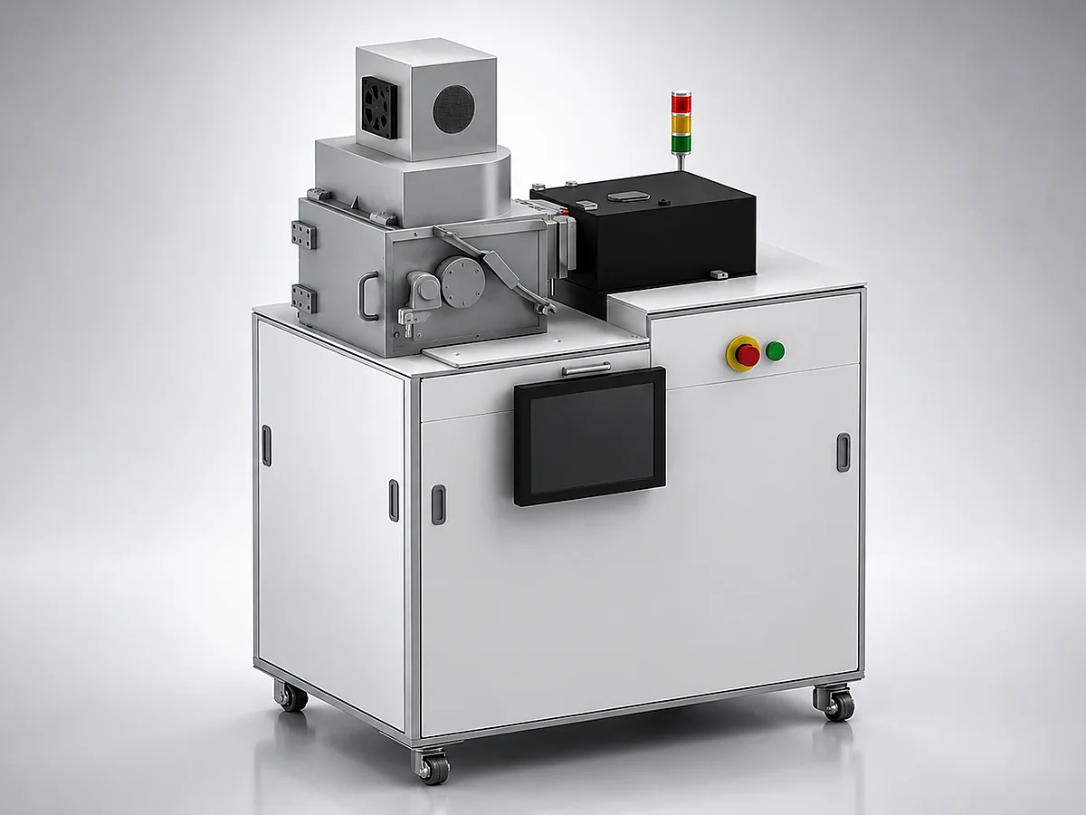
Wafer Size
4-12 in
Wafer Temp
20 to 400 °C
Uniformity
<1%
Precursor
2-6 lines
Process-first configuration
ALD selection starts with precursor chemistry, purge efficiency, temperature window, nucleation behavior, aspect ratio, plasma-assist requirements, and target film properties. The platform is configured around those self-limiting process constraints.
Atomic-layer control for Al2O3, HfO2, TiO2, and related oxide films used in gate dielectric and passivation research.
High step coverage for high-aspect-ratio structures, MEMS devices, porous materials, and complex research substrates.
Optional remote plasma supports lower-temperature process windows and additional material chemistries.
Core Process Windows
Sequential precursor exposure and purge cycles support atomic-scale thickness control and repeatable growth-per-cycle.
The ALD process is built for coverage inside high-aspect-ratio, porous, or non-planar features where line-of-sight deposition struggles.
Thermal ALD and optional PEALD let engineers tune temperature, reactivity, and film properties around substrate limits.
Technical Specifications
Review core platform capabilities for initial process planning. Our engineering team will confirm the final precursor and plasma configuration during quote review.
Applications
Gate dielectrics
Passivation layers
MEMS coatings
Energy storage materials
Optical coatings
2D material devices
Research evidence
Related Resources
FAQ
Atomic layer deposition builds films through sequential, self-limiting surface reactions. Each cycle deposits a controlled layer, enabling precise thickness control, strong conformality, and high uniformity on complex 3D structures.
The ALD platform supports oxide, nitride, metal, and complex oxide process families including Al2O3, HfO2, SiO2, TiO2, TiN, TaN, Pt, Pd, W, Ru, and related research materials depending on precursor configuration.
Choose ALD when the process requires atomic-level thickness control, very high conformality, high-aspect-ratio coverage, or gate dielectric and passivation films on complex geometries. PECVD is typically better for higher-rate dielectric deposition when perfect conformality is less critical.
Request a quote
Share your target film, precursor needs, wafer size, thermal budget, aspect ratio, plasma requirements, and timeline.