ICP-RIE
Configured to your process — engineering quote
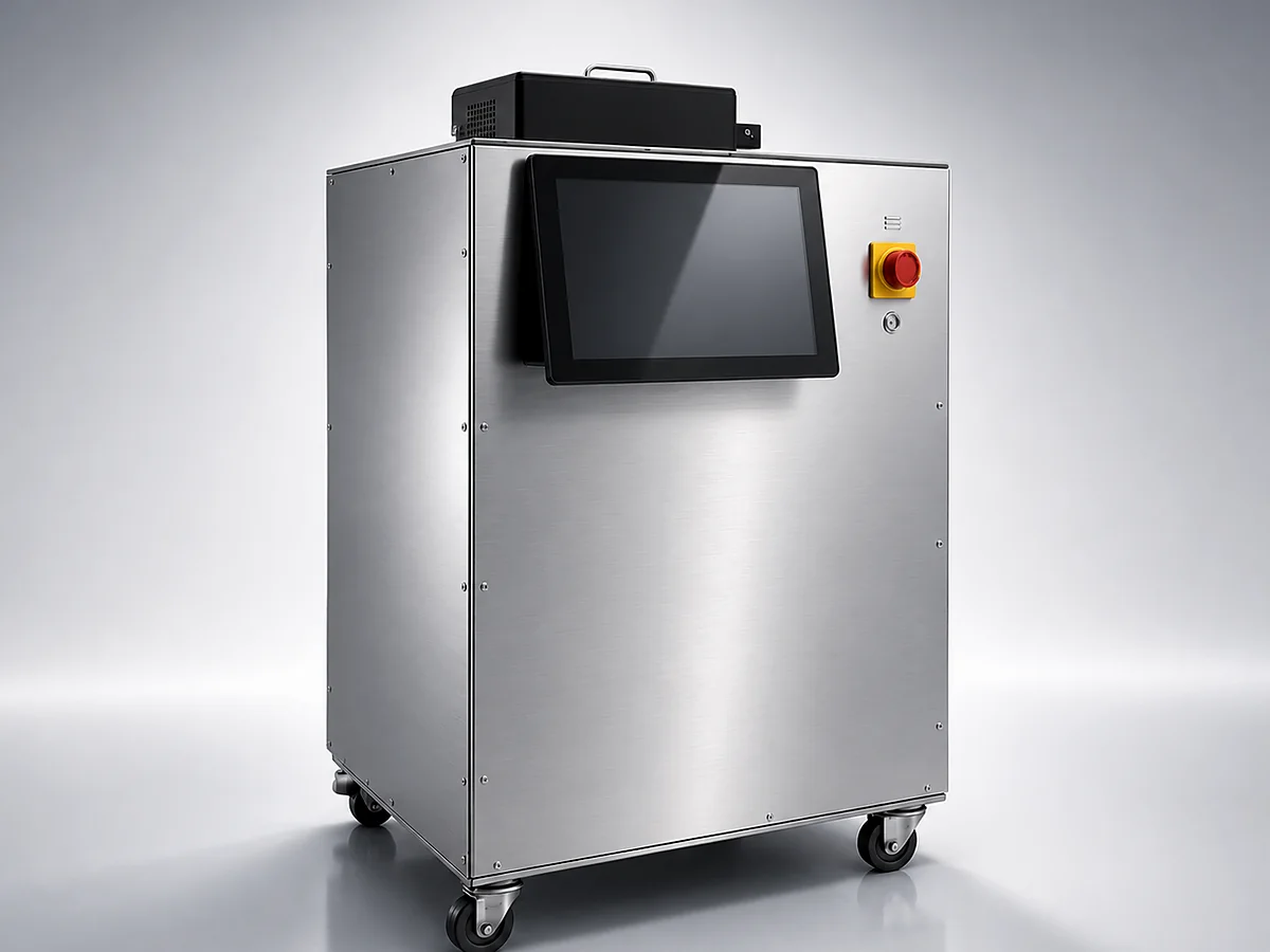
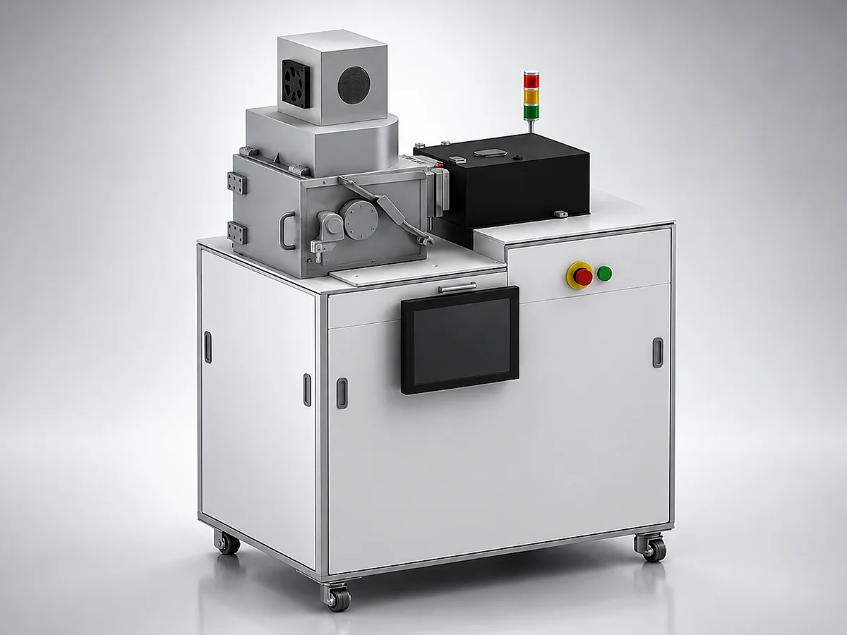
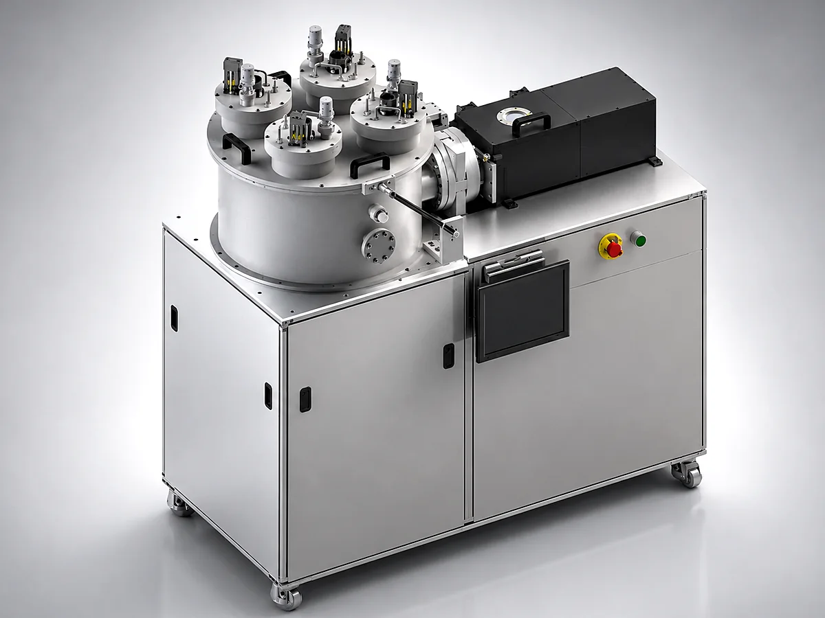
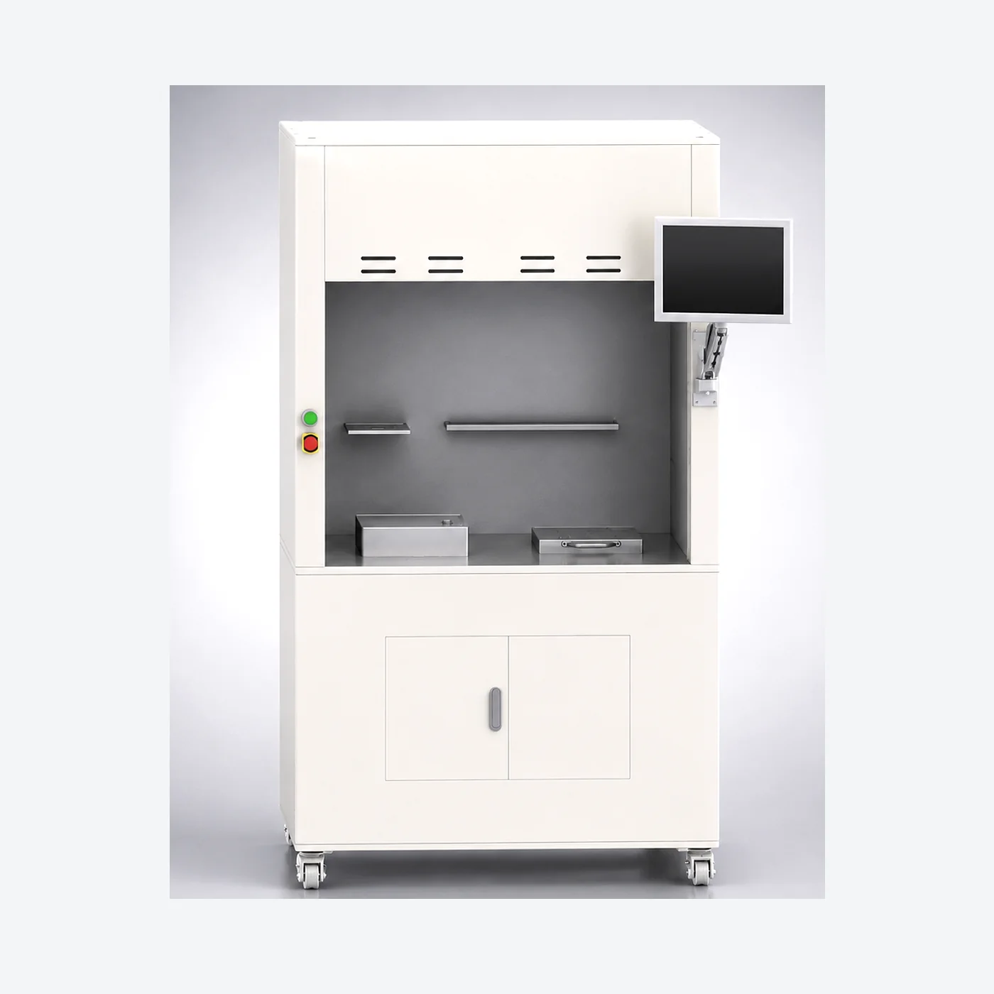
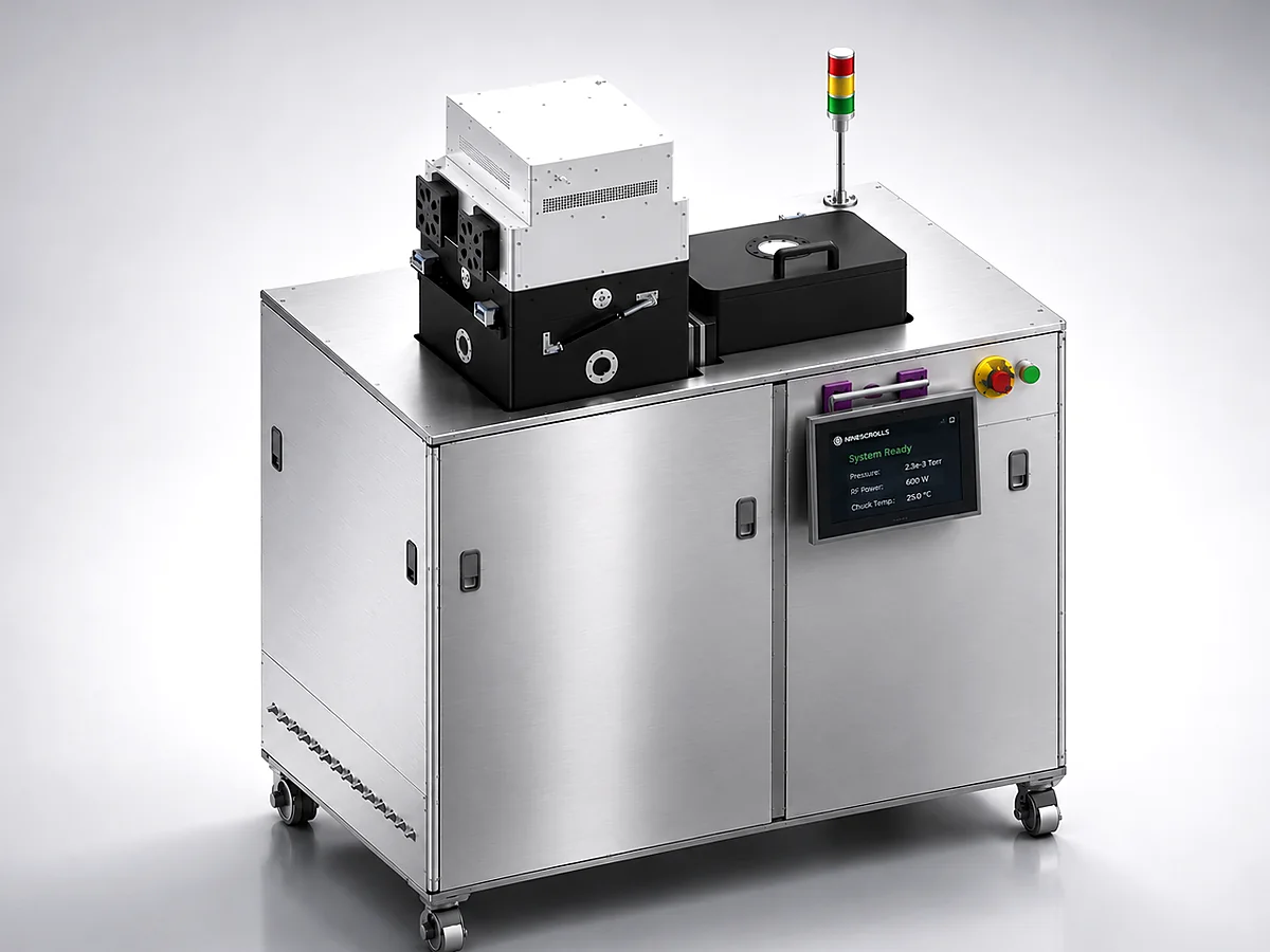
High-density plasma source for deep silicon etching, MEMS, diamond processing, and demanding anisotropy.
Browse NineScrolls systems by process capability, application fit, and purchasing path. RFQ platforms support custom configurations; plasma cleaners can be purchased online or quoted for institutional procurement.
Start with the process you need to run, then compare platform size, process role, purchasing path, and application fit.
Directional plasma and ion-beam systems for silicon, diamond, MEMS, photonics, compound semiconductors, and failure analysis.

Configured to your process — engineering quote
High-density plasma source for deep silicon etching, MEMS, diamond processing, and demanding anisotropy.

Configured to your process — engineering quote
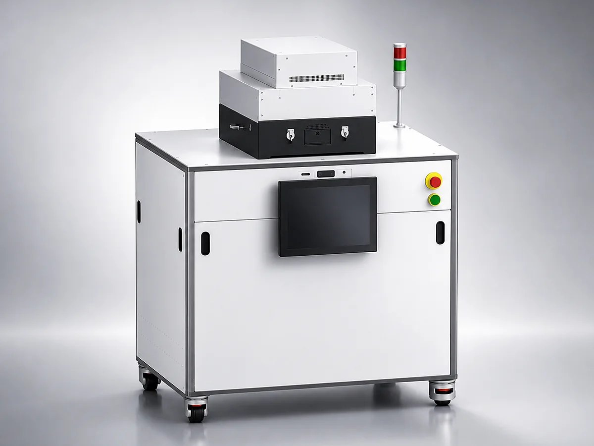
Reliable anisotropic plasma etching for universities, pilot labs, and surface activation workflows.

Configured to your process — engineering quote
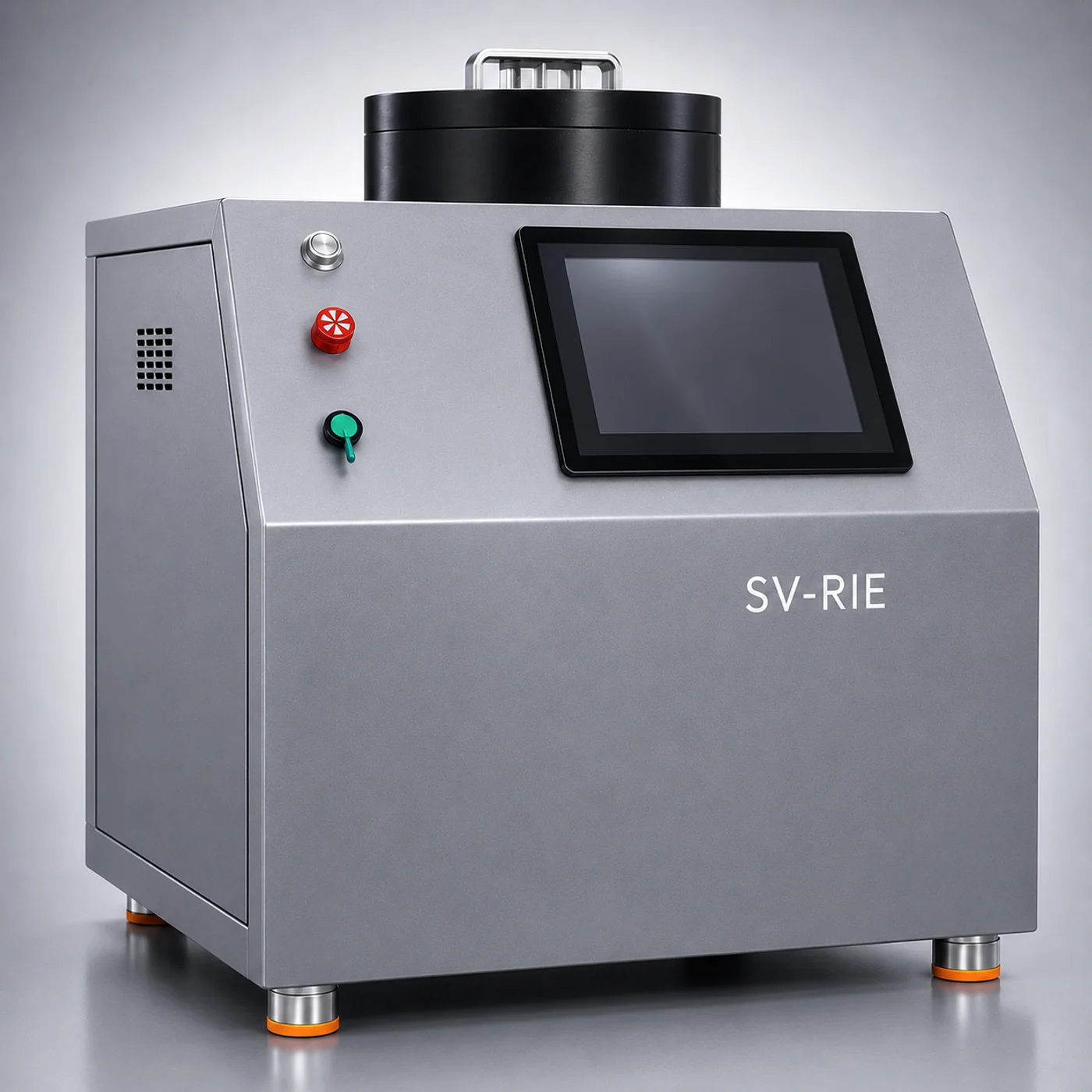
Benchtop reactive ion etcher for education, failure analysis, and small-lab process development.

Configured to your process — engineering quote
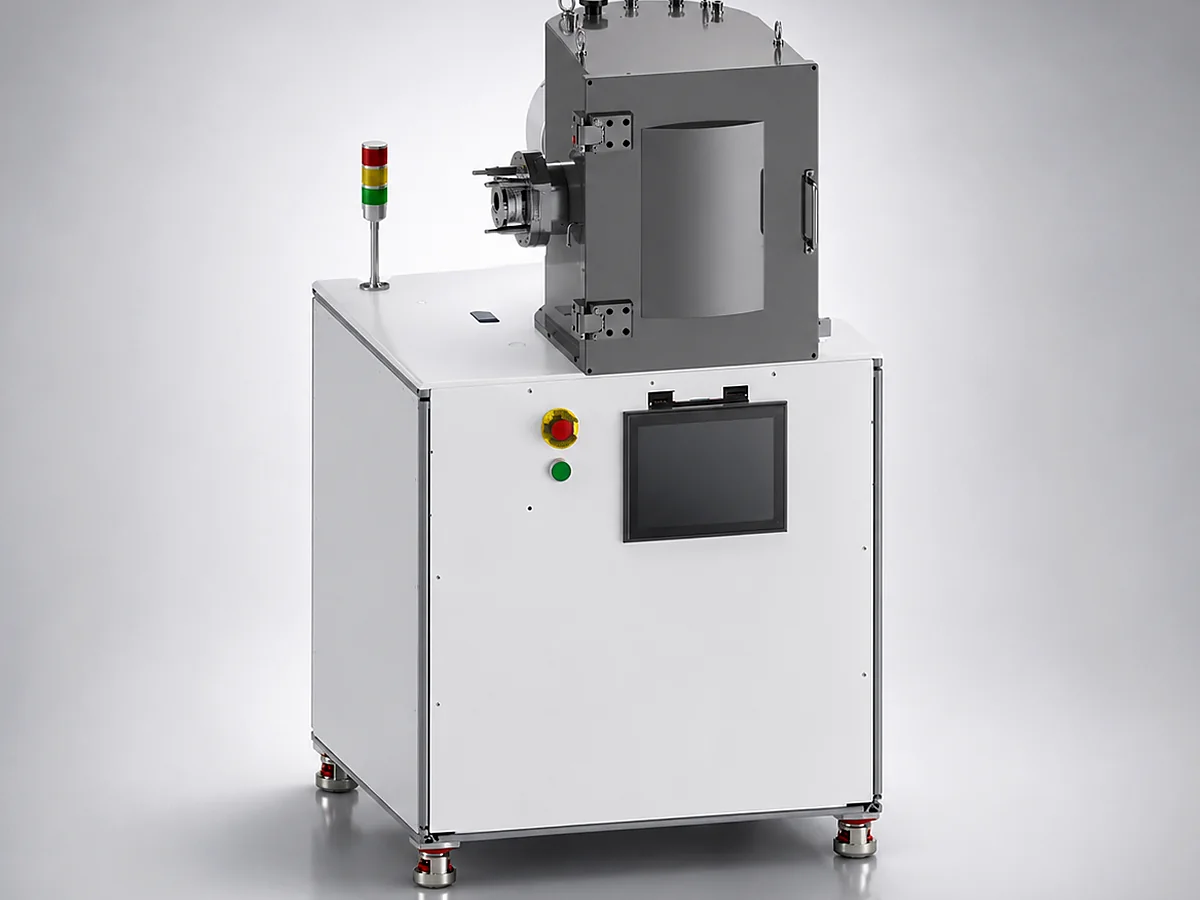
Ion beam milling for directional removal, hard masks, redeposition control, and precision angle etching.
PECVD, ALD, PVD, e-beam, and HDP-CVD platforms for thin films, dielectric stacks, optical coatings, and gap-fill processes.

Configured to your process — engineering quote
Plasma-enhanced thin-film deposition for dielectric films, passivation, and low-temperature stacks.

Configured to your process — engineering quote
Conformal ALD for nanolaminates, barrier layers, high-k dielectrics, and high-aspect-ratio structures.

Configured to your process — engineering quote
Magnetron sputtering for metals, oxides, nitrides, reactive sputter, and co-sputtered film stacks.

Configured to your process — engineering quote
High-density plasma CVD for gap fill, STI/IMD/PMD dielectric stacks, and advanced packaging.

Configured to your process — engineering quote
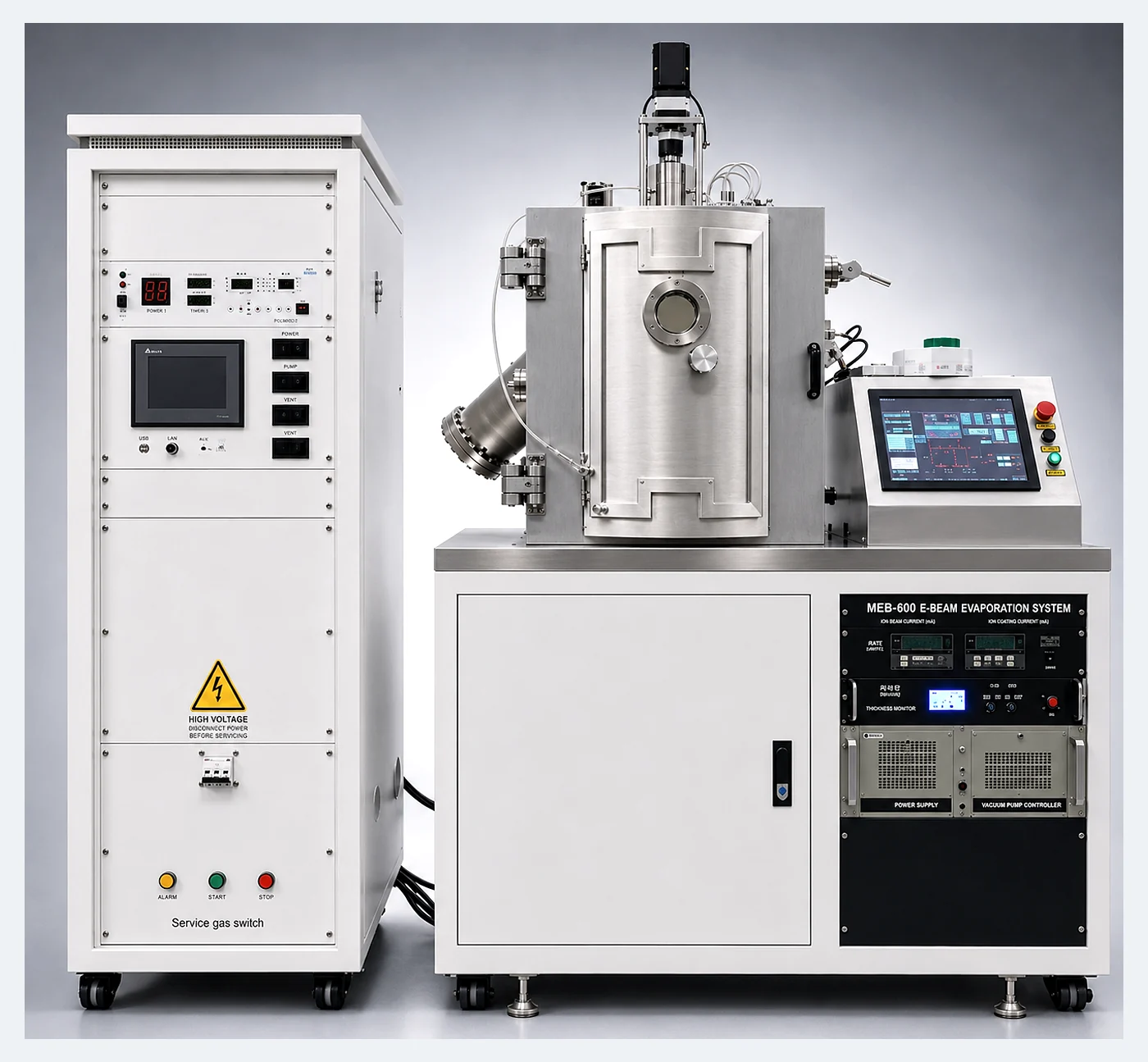
Multi-source e-beam and thermal evaporation for IR sensors, photonic crystals, and optical multilayers.
Coating, developing, bake, and resist-removal tools that support patterning workflows before and after etch or deposition.

Configured to your process — engineering quote
Spin coating, developing, bake, HMDS, EBR, and PEB modules for photolithography preparation.

Configured to your process — engineering quote
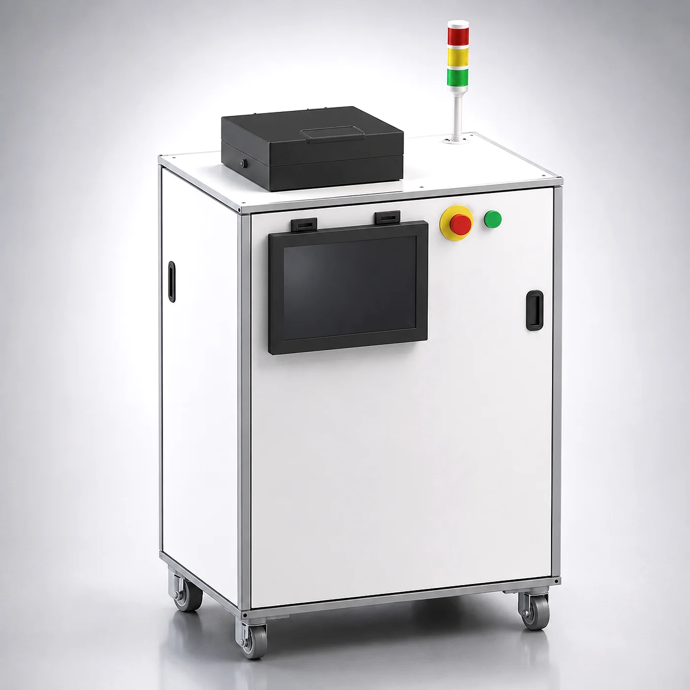
Plasma photoresist stripping and ashing platform for post-lithography resist removal.
Buy-online plasma cleaners for surface activation, bonding prep, sample cleaning, and routine laboratory workflows.

Standard configuration — buy online or request a quote
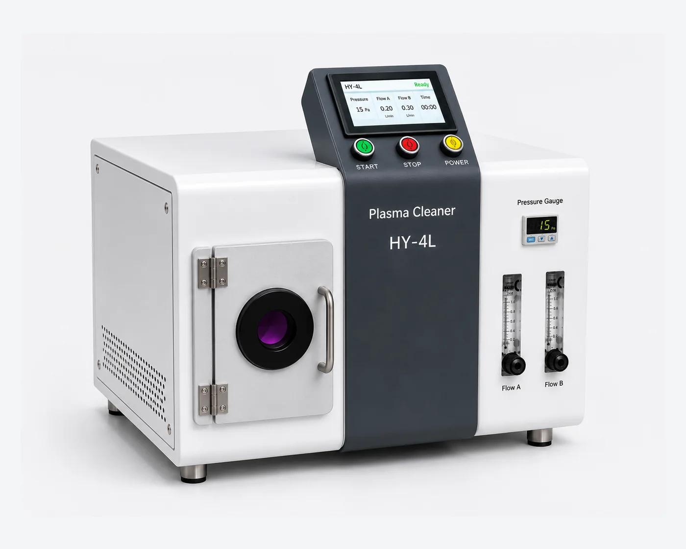
Compact plasma cleaner for sample preparation, teaching labs, bonding prep, and low-volume research.
Mid-Frequency (40 kHz) $6,499 · RF (13.56 MHz) $7,999

Standard configuration — buy online or request a quote
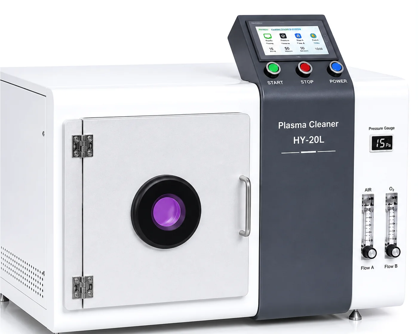
20-liter batch plasma processing for surface activation, bonding prep, and repeatable lab cleaning.
Mid-Frequency (40 kHz) $11,999 · RF (13.56 MHz) $14,999

Standard configuration — buy online or request a quote
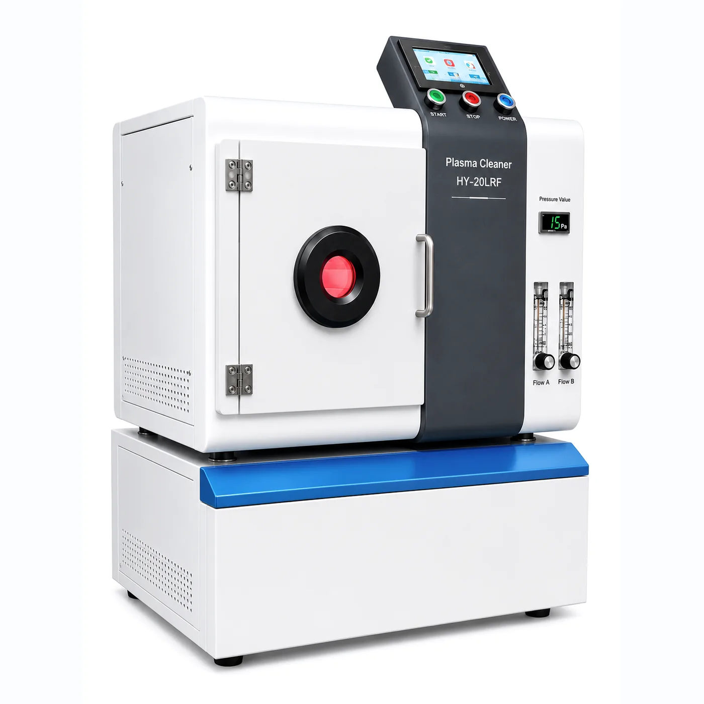
Research-grade 20 L RF plasma cleaner with tray-based processing and documented repeatability.

Standard configuration — buy online or request a quote
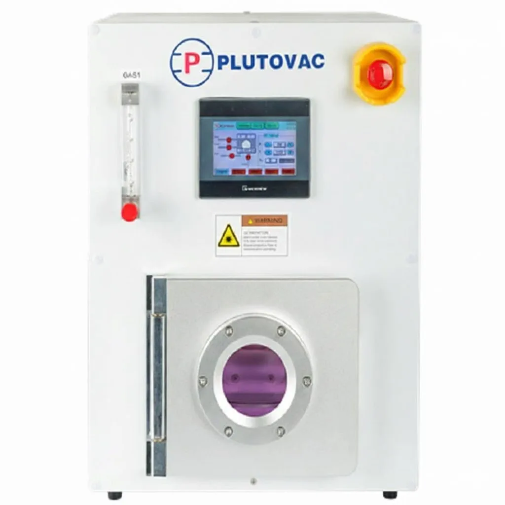
Compact RF plasma cleaner with touchscreen control for activation, cleaning, and surface preparation.

Standard configuration — buy online or request a quote
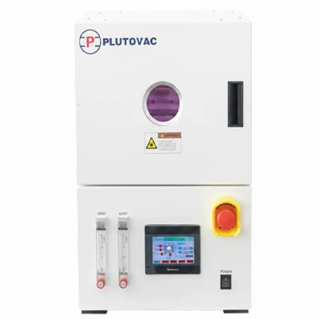
Mid-size RF plasma cleaner for larger fixtures, small batch work, and routine lab preparation.

Standard configuration — buy online or request a quote
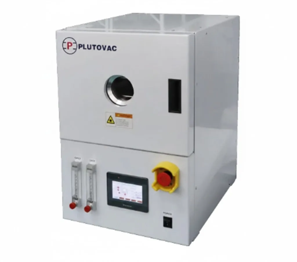
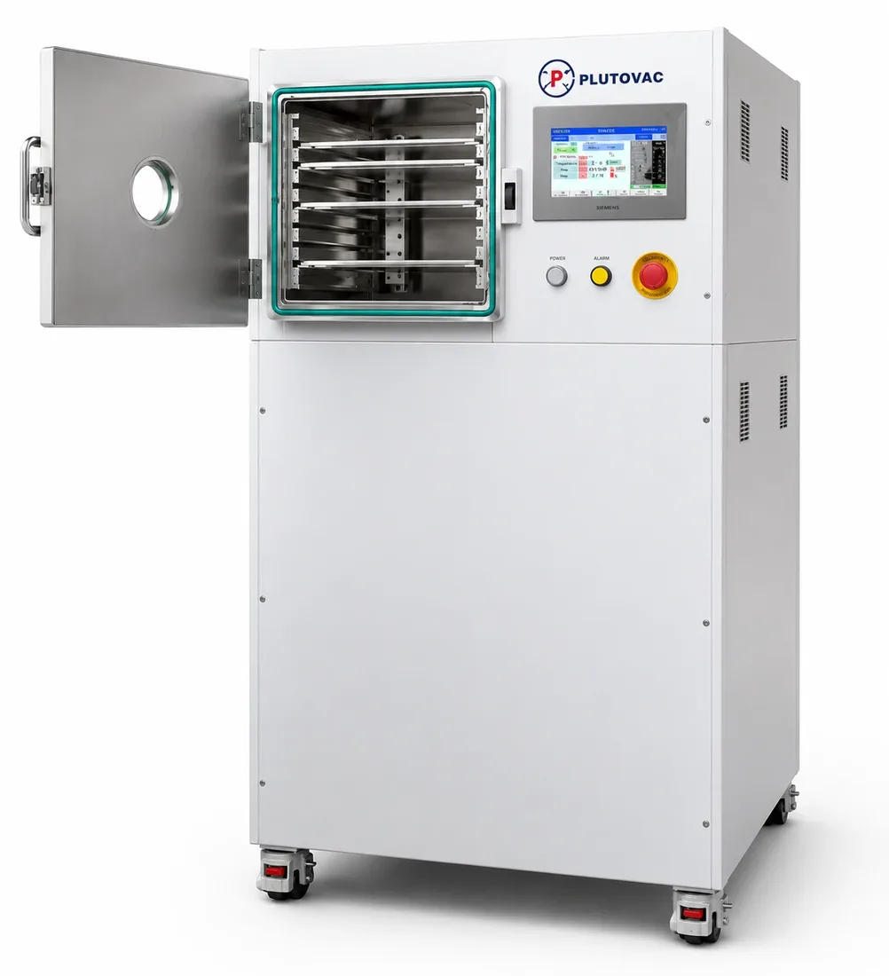
Flagship RF plasma cleaner with a 6061-T6 chamber and 0-500 W of RF power for advanced labs.

Configured to your process — engineering quote
Floor-standing 30L RF plasma system with one to four electrode pairs and two mass flow controllers for batch cleaning, activation, and surface treatment.
Manual, semi-automatic, automatic, and fully automatic platforms, with application pathways for low-temperature and vacuum probing, and silicon photonics probing.
Engineers usually evaluate by process first, then platform size, substrate, chemistry, and procurement path. These requirements help narrow the right equipment family and system configuration.
Need anisotropy, profile control, deep silicon, diamond, or ion milling? Start with ICP-RIE, RIE, Compact RIE, or IBE/RIBE.
Need dielectric films, conformal ALD, PVD metals, optical stacks, or gap fill? Start with PECVD, ALD, Sputter, E-Beam, or HDP-CVD.
Need coating, developing, bake, stripping, or resist removal around lithography? Start with Coater/Developer or Striper.
Need surface activation or lab-scale plasma cleaning? Start with HY and PLUTO buy-online platforms.
Need electrical, cryogenic, or wafer-level photonics characterization? Start with the wafer probe station selection hub.
Share your material stack, wafer size, process goal, and timeline. NineScrolls can help narrow the platform family before configuration review.