

Target Readers: Semiconductor/packaging process engineers, equipment engineers, PIs/lab managers, R&D procurement teams, and technical decision-makers.
TL;DR Summary
HDP-CVD enables high-density thin films and superior gap-fill in high-aspect-ratio (HAR) trenches/voids through a combination of high-density plasma and ion-assisted deposition. It is particularly effective for STI, PMD/IMD dielectric layers, TSV, advanced packaging, and MEMS. Compared with conventional PECVD, HDP-CVD achieves better void suppression and film density; compared with ALD, HDP-CVD offers higher throughput and lower cost-of-ownership (when requirements are met).
1) What is HDP-CVD?
HDP-CVD (High-Density Plasma Chemical Vapor Deposition) is a thin film deposition technology operating at low pressures (typically <10 mTorr), using high-density plasma (commonly ICP: Inductively Coupled Plasma) to enhance chemical reactions and physical re-sputtering. The core principles are:
- Generate high-density plasma, supplying abundant radicals to accelerate precursor decomposition and film formation;
- Apply bias power to introduce directional ion bombardment, enabling simultaneous deposition and re-sputtering, which improves sidewall/bottom coverage inside trenches and prevents keyholes/voids;
- Achieve high-density, low-defect dielectric films (SiO₂, SiNₓ, SiON, SiC, etc.) at relatively low substrate temperatures.
Common precursor/gas chemistries:
- SiO₂: TEOS/O₂/Ar or SiH₄/O₂(/N₂O)
- SiNₓ/SiON: SiH₄/NH₃/N₂(/N₂O)
- SiC: SiH₄/CH₄(/H₂/N₂)
2) How It Works (Why HDP Works)
- Chemical Deposition (CVD): Precursors decompose/react near the substrate to form solid films.
- Plasma Activation: High-density plasma generates abundant ions/radicals, lowering activation energy and enabling high-quality deposition at lower temperatures.
- Ion-Assisted Re-sputtering: Substrate bias accelerates ions toward the surface, lightly etching/re-distributing material so it migrates/fills trench bottoms, improving step coverage and gap-fill.
Analogy: It works like painting while smoothing at the same time — deposition "paints" the surface, while ions "smooth" excess material into gaps.
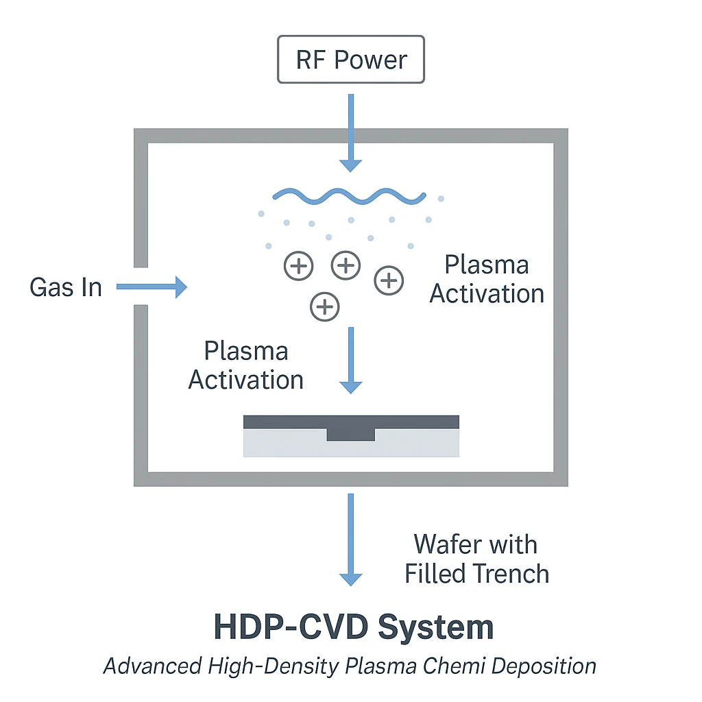
Figure 1: HDP-CVD Process Flow Diagram - Showing plasma generation, ion bombardment, and film deposition mechanisms
3) Comparison with Mainstream Deposition Routes
| Technology | Temp | Pressure | HAR Fill Control | Film Density | Throughput | Typical Applications |
|---|---|---|---|---|---|---|
| HDP-CVD | 200–450 °C | ~1–10 mTorr | Excellent (gap-fill) | High | Medium–High | STI, PMD/IMD, TSV, advanced packaging, MEMS |
| PECVD | 200–400 °C | ~0.1–3 Torr | Moderate | Moderate | High | Passivation, dielectric layers, H-doped films |
| LPCVD | 400–800 °C | ~0.1–1 Torr | Moderate | High | High | Poly-Si, SiNₓ, high-temp layers |
| ALD | 80–350 °C | Near vacuum pulsing | Best (atomic-level) | High | Low | Ultra-thin, ultra-uniform, gate oxides |
Rules of Thumb:
- For deep trenches, void-free, high-density films with higher throughput, use HDP-CVD;
- For extreme HAR or sub-10 nm ultra-uniform layers, ALD is preferred;
- For general coverage with cost sensitivity, PECVD is sufficient.
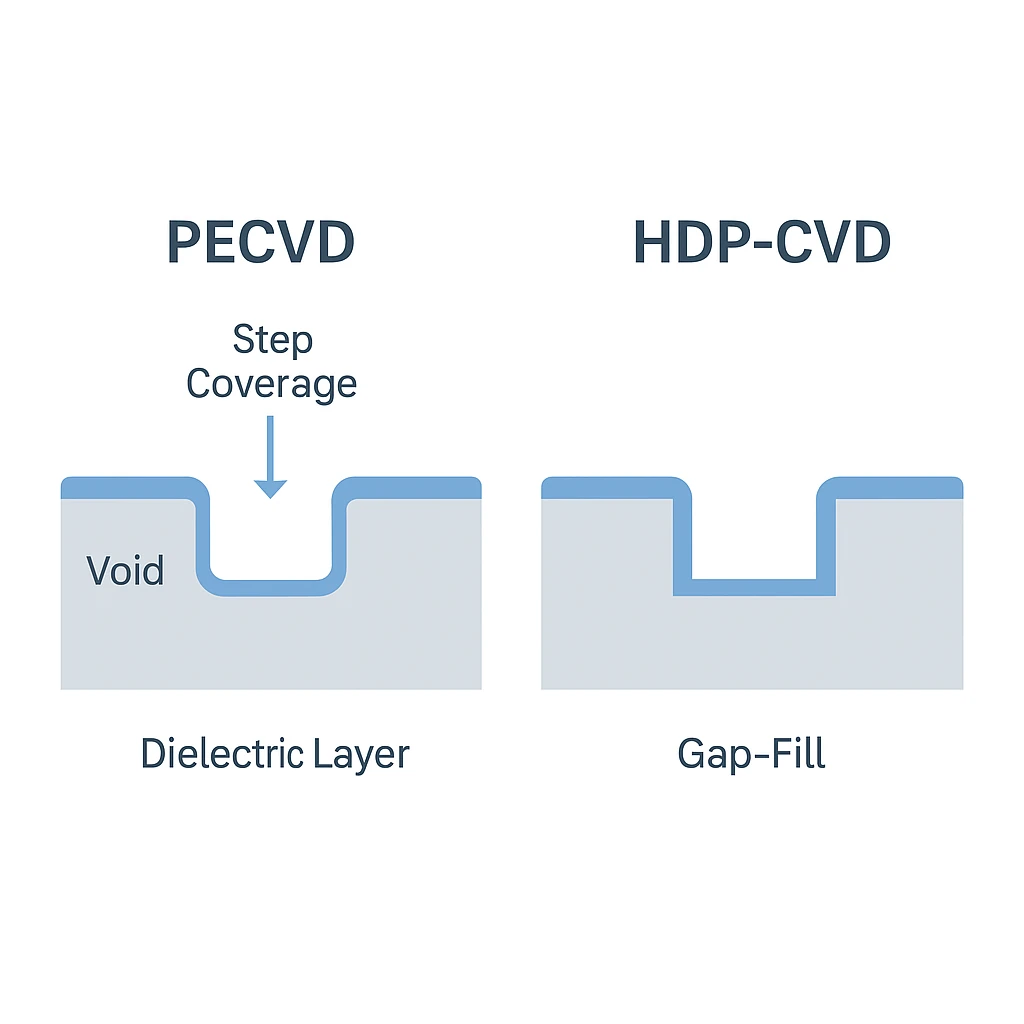
Figure 2: PECVD vs HDP-CVD Gap-Fill Comparison - Demonstrating performance differences between the two technologies in high-aspect-ratio trenches
HDP-CVD (Direct Plasma) vs Remote / Downstream Plasma CVD
A frequent point of confusion when comparing deposition tools is the difference between a conventional HDP-CVD reactor and systems that use remote (downstream) or pseudo-remote plasma control. The distinction is not the plasma chemistry — it is where the plasma sits relative to the wafer, and therefore what actually reaches the film surface.
- Direct high-density plasma (conventional HDP-CVD): the ICP source sustains a dense plasma (10¹¹–10¹² cm⁻³) directly above the wafer, and the wafer sits inside it. The surface receives radicals and a substantial, bias-controllable ion flux. That simultaneous deposition + ion sputter component is precisely what enables bottom-up gap-fill and high film density — and also what creates plasma-damage risk on sensitive devices.
- Fully remote / downstream plasma: the plasma is generated in a separate source region; ions and electrons largely recombine in transit, so predominantly neutral radicals reach the wafer. Deposition is gentle and virtually damage-free, but there is no ion-assist knob: no bias-driven densification, no sputter component, and therefore no HDP-class gap-fill. Deposition rates are typically lower.
- Pseudo-remote plasma control: an intermediate architecture — the plasma is displaced or confined away from the wafer (by source-to-wafer distance, grids, or magnetic confinement) without being fully remote. A reduced, tunable ion flux still reaches the surface. This trades away some gap-fill and densification capability in exchange for much lower damage, sitting deliberately between the two extremes.
| Attribute | Direct HDP-CVD | Pseudo-Remote Plasma | Fully Remote / Downstream |
|---|---|---|---|
| Ion flux at wafer | High, bias-controlled | Reduced, partially tunable | Negligible (radicals only) |
| Gap-fill (HAR trenches) | Excellent (dep + sputter-etch) | Moderate | Poor — conformal/flowable only |
| Film density / densification | High (ion bombardment) | Medium | Lower; may need post-anneal |
| Plasma damage risk | Highest — mitigate via bias/pulsing | Low–moderate | Minimal |
| Typical use | STI/PMD/IMD gap-fill, TSV, dense dielectrics | Damage-sensitive deposition needing some ion assist | Passivation on fragile devices, radical treatments, surface nitridation/oxidation |
Practical guidance: if the structure demands void-free filling of high-aspect-ratio gaps or maximum as-deposited film density, only a direct-plasma HDP-CVD architecture provides the bias-driven sputter component that makes it possible. If the device is damage-limited (thin gate stacks, III-V surfaces, MEMS with exposed sensitive layers) and the film is planar or conformal, a remote or pseudo-remote configuration — or PECVD with soft-landing recipes — is usually the better tool match. Evaluate candidates by asking one question first: does this film need ion bombardment to meet spec? The answer determines the architecture class before any other selection criterion applies.
4) Key Metrics & Influencing Factors
- Gap-fill capability: Influenced by bias power, source power, pressure, Ar/O₂ ratio, substrate temp;
- Film stress: Higher ion energy introduces more stress; optimized via temp control, bias/source ratio, gas composition;
- Refractive index/density/dielectric constant: Dependent on precursor chemistry (TEOS vs SiH₄), plasma energy, post-treatment;
- Charge/plasma damage: Mitigated by pulsed bias, soft-landing, and shielding.
5) Typical Applications
- STI (Shallow Trench Isolation): Void suppression, CMP compatibility — paired with reactive ion etching to define the trench profile.
- PMD/IMD Dielectrics: Denser insulation, reduced leakage, improved reliability;
- TSV/Advanced Packaging/Flip-Chip: Dielectric gap-fill and passivation downstream of DRIE Bosch via etching;
- MEMS/Sensors: Dielectric deposition/encapsulation above structures;
- Power Devices/Compound Semiconductors: High-quality dielectrics for high-voltage/temperature.
6) Starter Process Window (Example, Non-Production Recipe)
Ranges vary by tool/film target; baseline starting points:
- Pressure: 1–10 mTorr
- Substrate Temperature: 200–450 °C
- RF Source Power: 1.0–3.0 kW
- Substrate Bias: 300–1000 W
- Gas Chemistry:
- SiO₂ (TEOS/O₂/Ar): Ar improves directional re-sputtering;
- SiO₂ (SiH₄/O₂/N₂O): Higher rate, but watch H-content/stress;
- SiNₓ (SiH₄/NH₃/N₂): Adjust N/H ratio, refractive index.
DOE Tip: Use Source/Bias/Pressure as 3-factor matrix, verify via SEM (gap-fill) + wafer bow (stress).
7) Equipment Selection Checklist
- Chamber design: Single/multi-chamber, replaceable liners, electrode temperature control;
- RF System: Source/bias range, matching network speed, pulsed/modulated capability;
- Temperature Control: Independent electrode/wall heating, reduce particles/defects;
- Gas Delivery: Multi-zone MFCs, precursor heating/TEOS bubbling stability;
- Vacuum System: Dry pump + turbo, low-pressure stability, fast pump-down;
- Wafer Handling: Open-Load vs Load-Lock (throughput, cleanliness);
- Monitoring & Traceability: Chamber pressure/RF/temp/flow logged for SPC;
- Safety Compliance: Toxic/flammable gas interlocks, abatement, NFPA/local codes.
8) Facility & EHS Notes
- Precursors/Gases: TEOS, SiH₄, NH₃, CH₄, O₂, Ar, N₂; (SiH₄/NH₃ = flammable/toxic, requires gas cabinets, detection, interlocks);
- Exhaust Abatement: Dry/wet/combustion scrubbers (per chemistry);
- Safety: Blast panels, interlocks per regulations;
- Training: Standardized operation, maintenance, emergency SOPs.
9) Maintenance & Cost of Ownership (CoO)
- Replaceable liners/electrodes reduce particles/cleaning frequency;
- Plasma clean recipes + periodic wet cleans;
- Consumables: liners, O-rings, MFC filters, pump oil;
- Downtime scheduling aligned with fab/lab planning;
- CoO includes gases/precursors, consumables, pumps, utilities.
10) Metrology & Validation
- Thickness/uniformity: Ellipsometry, XRR;
- Composition/bonding: FTIR, XPS;
- Density/stress: Wafer bow, refractive index benchmarking;
- Structural: Cross-section SEM/TEM (gap-fill, voids);
- Electrical: CV, leakage, breakdown strength.
11) Common Issues & Troubleshooting
| Issue | Possible Cause | Quick Fix |
|---|---|---|
| Voids in trench | Low bias, high pressure, low Ar | Increase bias, lower pressure, add Ar, adjust source/bias ratio |
| Excess stress/wafer bow | High ion energy, temp instability | Lower bias, split deposition steps, improve electrode temp control |
| Particles/rough surface | Dirty chamber, insufficient cleans | Increase cleaning, check liner wear |
| Refractive index/composition drift | MFC drift, unstable precursor | Calibrate MFC, check TEOS heating/stability |
| RF/matching instability | Matching box/cable/ground issues | Inspect matching unit, RF cabling, grounding |
12) NineScrolls HDP-CVD Highlights
- Compact uni-body design (~1.0 m × 1.5 m footprint);
- Multi-material compatibility: Si, SiO₂, SiNₓ, SiON, SiC;
- RF Options: Source 1000–3000 W / Bias 300–1000 W;
- Electrode & liner temp control: Stress tuning, contamination control;
- Multi-zone gas lines: 6 standard, customizable;
- Wafer handling: Open-Load or Load-Lock;
- Excellent step coverage/gap-fill, tunable for stress & dielectric performance;
- Modular upgrades: Balance performance vs cost.
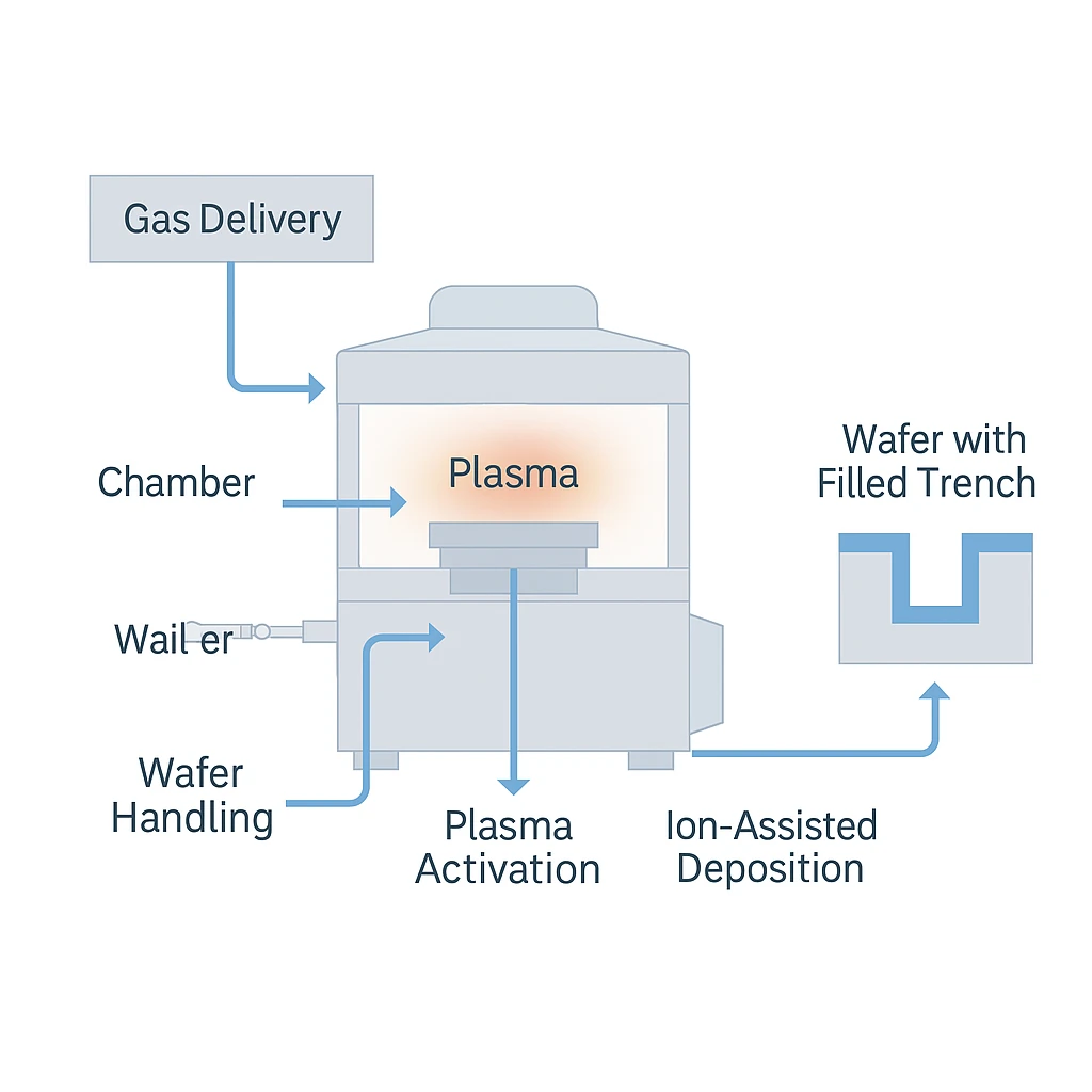
Figure 3: NineScrolls HDP-CVD System Modular Structure - Showing chamber design, RF systems, gas delivery, and control modules
Product page: https://www.ninescrolls.com/products/hdp-cvd
13) Purchasing & Pilot Line Workflow
- Define targets: CD/HAR, dielectric specs (σ, n/k, leakage);
- Facility check: Power, cooling, CDA, exhaust/abatement, gas cabinets;
- Configuration list: RF source/bias, temp, gas/precursors, handling;
- Test wafer plan: DOE design + metrology (SEM/FTIR/stress/electrical);
- Acceptance: Void-free fill, stress range, uniformity/repeatability, SPC;
- EHS/SOP: Hazard approval, operator/maintenance training, emergency response.
14) FAQ
Q1: Will HDP-CVD damage devices due to plasma?
A: Mitigate with lower bias, pulsed/segmented processes, soft-landing, grounding/shielding.
Q2: How does CoO compare to PECVD?
A: Higher RF/chamber complexity, but better gap-fill and higher throughput make CoO competitive.
Q3: Is TEOS mandatory?
A: No. SiH₄/O₂(/N₂O) gives higher rates but requires balance of H-content, stress, dielectric properties.
Q4: How to manage stress in multilayers?
A: Alternate low/medium bias, gas ratio/temp tuning, plus anneal/plasma post-treatment.
Q5: How does HDP-CVD differ from remote (downstream) plasma CVD?
A: In HDP-CVD the wafer sits inside a dense plasma and receives both radicals and a bias-controlled ion flux — enabling bottom-up gap-fill and dense films, at the cost of plasma-damage risk. In remote/downstream systems the plasma is generated away from the wafer and mostly neutral radicals arrive, giving damage-free but slower, non-gap-filling deposition. Pseudo-remote designs sit in between, with a reduced, tunable ion flux. Choose by whether the film needs ion bombardment (gap-fill, densification) or must avoid it (damage-sensitive devices).
15) Glossary
- HAR: High-Aspect-Ratio structure;
- Gap-fill: Ability to fill voids/trenches;
- ICP: Inductively Coupled Plasma;
- Bias: Substrate bias power, controls ion energy;
- TEOS: Tetraethyl Orthosilicate;
- SPC: Statistical Process Control.
Call-to-Action
- Need test recipes and DOE templates for your structures/materials? Contact our process team.
- Want configuration and budget recommendations? We provide facility checklist and tool selection guidance.
Contact:
Product page: https://www.ninescrolls.com/products/hdp-cvd | Email: info@ninescrolls.com | Online technical consultation available
References
- Vassiliev, V. Y., et al. "Trends in void-free pre-metal CVD dielectrics." Solid State Technology, 44(3), 129 (2001).
- Nguyen, S. V. "High-density plasma chemical vapor deposition of silicon-based dielectric films for IC applications." IBM Journal of Research and Development, 43(1.2), 109–126 (1999). doi:10.1147/rd.431.0109
- Chiang, C., et al. "High-density plasma CVD oxide gap-fill." Thin Solid Films, 313–314, 506–511 (1998). doi:10.1016/S0040-6090(97)00872-6
- SEMI Standard E112: Guide for Measuring Dielectric Film Thickness and Uniformity. semi.org