What Changed
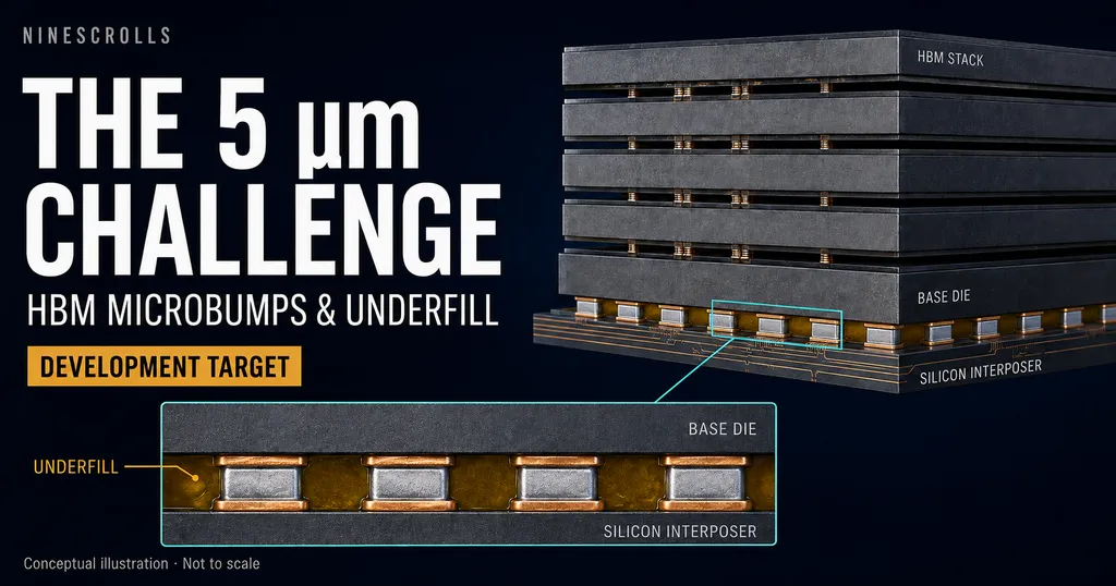
On September 2, 2026, materials-industry sources reported that TSMC has asked its materials and equipment partners to develop bonding and underfill solutions for roughly 5 µm-class microbumps, rather than moving the HBM-to-interposer interface to copper hybrid bonding. Korean and Japanese supply chains have already begun development work. Reported mass-production timing differs between accounts of the same report — the second half of 2027 in one, the second half of 2028 in another — so treat the date as unsettled.
The decision is not a retreat from density. It is a decision to buy density out of bump height instead of out of a new joining mechanism. HBM4 bumps are around 10 µm today; the request is to halve that while keeping solder, underfill, reflow, and the entire inspection and rework infrastructure that already qualifies at volume.
Separately, SK hynix presented at Hot Chips 2026 a roadmap that keeps microbump-based MR-MUF through HBM4 and HBM4E, deferring direct bonding to HBM5 and beyond 20-layer stacks. Foundry and memory have converged on the same answer for the same generation.
The Bump-Height Ladder: 25 µm to 5 µm Under a Fixed Ceiling
The driver is a ceiling that does not move. JEDEC's JESD270-4 HBM4 standard caps cube height at 775 µm — itself already a relaxation from the 720 µm that held through HBM3E. Every additional DRAM layer, and every additional I/O contact, has to be found inside that budget.
The reported height progression: 15–25 µm for HBM3E, approximately 10 µm for HBM4, and 5 µm as the development target beyond it. SK hynix's disclosed HBM4 figures show what is being packed into the same envelope — more than 20,000 TSVs and 16,148 base microbumps in a 12.8 × 11 mm part, targeting over 2 TB/s and a 40%-plus power-efficiency gain, with 12-high in mass production and 16-high in qualification.
Two interfaces are shrinking at once. Memory vendors thin dies and tighten die-to-die gaps inside the stack; TSMC must simultaneously lower the bumps that attach the finished cube to the silicon interposer, because accelerator-side contact counts keep climbing. The interposer side of that geometry is covered in our guide to the 2.5D TSV interposer as a lateral routing layer, and the vertical path through the stack in our through-silicon via guide.
The Bottleneck Is the Underfill, Not the Bump
The most useful line in the report is a materials-supplier assessment: sub-15 µm bumps already exist, but quality assurance below 15 µm remains difficult, and the harder problem is developing an underfill that can guarantee them — not the bumps themselves. Japanese materials suppliers have previously stated they cannot warrant quality below 15 µm. A 5 µm bump sits well beneath that threshold.
At 5 µm the three requirements collide: void-free underfill flow into a gap a fraction of its current height, residual flux control at a volume where a single trapped void spans multiple joints, and placement alignment tight enough that the joint lands. That combination is why the request is understood to have been distributed across several materials and equipment partners rather than sole-sourced.
Note what this makes the underfill: not a protective encapsulant applied after the interconnect works, but a co-limiting process step. A film-type or capillary underfill that cannot wet a 5 µm gap without voiding caps the interconnect regardless of how well the bumps are formed. The thermomechanical consequences of that gap — CTE mismatch across the stack, warpage in thinned dies, fatigue at the joints — are the subject matter of our 3D packaging reliability guide.
Why Hybrid Bonding Did Not Take This Slot
Hybrid bonding removes bumps entirely and joins polished copper pads in a dielectric field. It is in high-volume production on logic. It did not win the HBM interface this cycle for reasons reported in late August 2026 as process-control rather than economic ones.
Two constraints were named. First, thermal budget: HBM needs deposition and anneal below the 300–350 °C range typical of current hybrid-bonding flows, because DRAM refresh characteristics degrade under that heat. Second, CMP: the copper pad recess that determines whether pads expand into contact during anneal must be held to roughly 5 nm dishing with copper surface roughness under 2 nm, and those numbers set the bond energy and shear strength directly.
Those are surface-preparation specifications, and they are the subject of our guide to CMP coplanarity, plasma activation, and pre-bond surface readiness in Cu-Cu hybrid bonding. The comparative case — at which pitch the bumpless route repays its process-control cost — is laid out in hybrid bonding versus micro-bump interconnect. TSMC's answer for the HBM-to-interposer joint, at HBM4's pitch, is that it does not yet.
Two Different Interfaces: SoIC Bonds, CoWoS Bumps
TSMC is not choosing between the two technologies company-wide. It already runs hybrid bonding in SoIC for logic-on-logic stacking while keeping microbumps in CoWoS for attaching HBM to the interposer. The same vendor uses both, because the two interfaces have different die thicknesses, different thermal budgets, different known-good-die economics, and different inspection and rework paths.
Inside the memory stack the split persists as well: SK hynix applies liquid underfill after mass reflow (MR-MUF), strong against thin-die warpage but higher in thermal resistance with a narrower gap-fill window; Samsung inserts a film underfill and thermocompression-bonds (TC-NCF), better on productivity and heat but more sensitive to chip warpage. Neither is being replaced for HBM4-generation product.
The general point — that bonding method is selected per interface against warpage, thermal budget, and yield, not adopted wholesale — is what our wafer bonding technologies hub exists to compare across fusion, adhesive, eutectic, thermocompression, and hybrid routes.
NineScrolls Niche Angle
Plasma processing. A deferred hybrid-bonding transition does not defer the etch work behind it. The 20,000-plus TSVs per HBM4 die are still deep silicon ICP etch, still backside reveal, still passivation — that volume grows with layer count regardless of how the cube attaches to the interposer. What the deferral does change is where plasma activation demand sits: activation is the step that makes room-temperature contact possible in a direct bond, so its ramp in memory now tracks HBM4E and HBM5 rather than HBM4.
Thin-film deposition. Two film requirements move in opposite directions. On the microbump path, the passivation and dielectric films around a 5 µm joint have to hold their thickness tolerance across a gap half its former height — a PECVD and ALD uniformity problem before it is a bumping problem. On the hybrid-bonding path, the reported sub-300 °C requirement is a direct constraint on deposition: bonding dielectrics for memory will have to be deposited and annealed at temperatures DRAM tolerates, which favors plasma-enhanced and atomic-layer routes over thermal ones.
Equipment supply chain. The signal for tool and materials suppliers is that the 5 µm microbump and the sub-300 °C hybrid bond are now parallel development programs, not sequential ones — a supplier cannot treat either as safely deferred. For university and R&D laboratories, the useful read is that the open questions named in this report are exactly the ones a lab-scale system can address: gap-fill and void behavior at reduced standoff, low-temperature dielectric quality, and surface preparation ahead of direct bonding. The CMP-dishing and roughness targets above are measurable on standalone equipment long before any of it reaches a production bonder.
Caveat. This story rests on unnamed materials-industry sources reported through trade press, not on a TSMC disclosure or a peer-reviewed result. The mass-production date is reported inconsistently. Treat the 5 µm figure as a stated development target, not a qualified specification.
Sources
- TSMC reportedly asks suppliers to develop 5μm HBM microbumps — DigiTimes, September 2, 2026
- TSMC to Keep Microbump for HBM Packaging for Now, Tasks Suppliers with 5μm Challenge — BigGo Finance, September 2, 2026
- HBM hybrid bonding delayed by 300°C heat and CMP dishing — DigiTimes, August 26, 2026
- SK hynix HBM Packaging at Hot Chips 2026 — ServeTheHome, August 23, 2026
- HBM4 Sticks With Microbumps, Postponing Hybrid Bonding — Semiconductor Engineering, January 13, 2026
- The current state of Hybrid Bonding in 2026 — Tom's Hardware, September 2, 2026