Surface Preparation for Cu-Cu Hybrid Bonding: The Conditioning Chain That Decides Yield
By NineScrolls Engineering · 2026-06-01 · 17 min read · Process Integration
Target Readers: Process and packaging engineers, yield engineers, and R&D teams working on Cu-Cu hybrid bonding for 3D integration, advanced memory, and CMOS image sensors.
This article focuses only on surface preparation. For the complete hybrid-bonding workflow — alignment, contact, anneal, and the bonder itself — see our Wafer Bonding Technologies Guide. For the fundamentals of plasma surface activation across materials, see our Plasma Surface Modification Guide. What follows is the one thing those two pages leave room for: the chain of surface-conditioning steps that decides whether a hybrid bond will actually take.
1. Why Surface Preparation Dominates Yield
A hybrid bond is only as good as the two surfaces brought together to make it. The aligner, the bonding tool, and the post-bond anneal all matter — but by the time the wafers touch, the outcome is largely already set. The surface state going into bonding is what decides whether the interface closes void-free, whether the copper pads actually merge, and how strong the finished bond is. Get the surface wrong and no amount of alignment accuracy or anneal optimization recovers it.
This is what makes hybrid bonding unforgiving in a way solder-bump packaging never was. A microbump tolerates a particle, a little oxide, a few nanometers of height variation — the solder reflows and absorbs it. A hybrid bond has none of that slack: the dielectric must touch dielectric across the whole wafer at room temperature, and the recessed copper must expand into contact on anneal. Both depend entirely on a surface that is flat, clean, activated, and free of copper oxide — to tolerances an order of magnitude tighter than any earlier method. Voids, weak joints, and opens almost always trace back to a surface that was out of spec before the wafers ever met. The rest of this guide walks that conditioning chain, step by step, and ends the moment the surface is ready to bond.
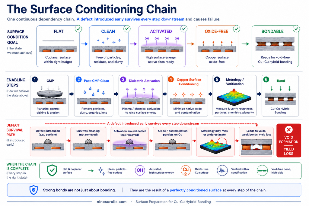
2. The Surface Conditioning Chain
Surface preparation for hybrid bonding is not a set of independent steps run in any order — it is a single dependency chain, where each step prepares the surface for the next and any defect introduced early survives everything after it. There are five links:
- CMP — planarize copper and dielectric into one coplanar surface, with the copper deliberately recessed a few nanometers.
- Post-CMP cleaning — remove slurry residue and particles before they become voids.
- Dielectric activation — raise the dielectric's surface energy by plasma so it bonds on contact at room temperature.
- Copper preparation — clear and keep the copper free of native oxide so the pads can interdiffuse on anneal.
- Metrology — verify roughness, recess, particles, and surface energy before committing to the bond.
Read top to bottom, the chain runs: a flat, dished surface (CMP) → a clean one (cleaning) → a bondable dielectric (activation) → bondable copper (copper prep) → a verified one (metrology) → bond. The sections that follow take each link in turn. Where a link fails, a specific defect appears at the interface — a mapping we return to in the final section.
3. CMP Requirements
CMP is the step that turns two dissimilar materials — copper pads and the surrounding dielectric, whether SiO₂ or SiCN — into one continuous, coplanar surface. That single plane is the precondition for everything that follows: hybrid bonding starts as dielectric-to-dielectric contact at room temperature, and that contact can only propagate across the wafer if the dielectric sits in one plane everywhere. The plane and the recess CMP leaves set the ceiling on the whole process — no later step recovers a surface left wavy or a recess left off-target.
Three things define an acceptable post-CMP surface.
Roughness. The dielectric must finish at sub-nanometer RMS — roughly below 0.5 nm. This is not a cosmetic target. Two surfaces brought into contact close by conforming to each other, and roughness sets how completely they can do so. Every nanometer of asperity is interface that never touches, and untouched interface is where bonding does not initiate. Roughness here puts a hard ceiling on bond coverage.
Coplanarity. Flatness has to hold at two scales at once. Globally, within-wafer non-uniformity must stay tight enough that center and edge present the same height; a wafer that is planar locally but bowed or thicker at the edge leaves whole annular regions that never make contact. Locally, at the die level, dishing across wide copper features and erosion of dense dielectric must stay bounded so no individual pad or field region falls out of plane. Either failure leaves a region that never touches — and a region that never touches is a void.
Copper recess. This is the crux. CMP does not finish the copper flush with the dielectric; it deliberately leaves the pads recessed a few nanometers below the dielectric plane. The logic follows from the bond sequence: the dielectric must mate first at room temperature, and only then does the copper, expanding on the post-bond anneal, close the remaining gap and merge pad-to-pad. (How that closure happens belongs to the bonding hub, not here.) The recess therefore has to land inside a narrow window. Too much recess and the copper cannot expand far enough to bridge the gap — the joint stays open. Too little, or copper left proud of the dielectric, and the pads prop the surfaces apart before the dielectric can mate — a void opens around them. That window is often only a couple of nanometers wide, and it has to hold not at one site but across the entire wafer, wafer to wafer, lot to lot.
The difficulty is that these three requirements share one operation: the removal that drives roughness down tends to deepen dishing, and the endpoint that controls recess at one pad density behaves differently at another. CMP for hybrid bonding is therefore tuned not for removal rate but to deliver a specific surface geometry, held to nanometer tolerances, uniformly, every wafer — the surface the next four links inherit.
4. Post-CMP Cleaning
CMP leaves a surface that is flat but filthy. The slurry that did the polishing leaves residue behind — abrasive particles, organic additives — along with loose particulates dislodged during the process and trace metal-ion and organic contamination smeared across both the copper and the dielectric. None of it is visible at the scale that matters, and all of it has to come off before the wafers meet.
The particle problem is the headline. On a hybrid bond a single sub-micrometer particle does not stay a local defect: it props the two wafers apart at its location, and the surfaces fail to close for a wide radius around it. A 1 µm particle can nucleate a void hundreds of micrometers across — orders of magnitude larger than the particle itself — swallowing many bond pads at once. This is why post-CMP cleaning is the single largest yield lever after CMP itself, and why hybrid bonding demands cleanliness well beyond what ordinary fab steps tolerate.
The workhorse is megasonic wet cleaning — high-frequency acoustic cavitation that lifts particles off the surface — paired with chemistry tuned to dissolve residue without attacking the copper or roughening the dielectric. The defining requirement is particle removal efficiency at the relevant size without re-deposition: a particle lifted off one site and dropped onto another is just as damaging as the one never removed, so the clean is judged on net particle count, not gross removal. Dry, plasma-assisted cleaning approaches complement the wet step where organic films resist liquid chemistry.
Contamination control matters chemically as well as physically. Organic residue or metallic contamination left on the dielectric suppresses the surface activation that comes next, capping how well the dielectric will bond; the same contamination on the copper interferes with pad-to-pad joining. A surface that passes the particle spec but carries chemical residue is still out of spec. Only a clean surface — particle-free and chemically uncontaminated — goes forward to activation.
5. Plasma Activation
A clean dielectric is not yet a bondable one. After cleaning, the SiO₂ or SiCN surface is flat and free of residue, but its surface energy is too low for two such faces to bond on contact at room temperature — bring them together and they touch without taking. Plasma activation closes that gap. It is the step that converts a clean surface into one that bonds spontaneously, and it is the difference between a chain that ends in a bond and one that ends in a wafer that simply will not stick.
The mechanism is surface-specific. A low-energy plasma — typically N₂, O₂, or H₂ chemistry — terminates the dielectric with reactive species, raising its surface energy and creating the dangling and –OH-type sites that let two faces form bonds the moment they meet. No high-temperature step is needed to initiate the bond: activation is what enables room-temperature dielectric bonding, with the interface strengthening later on anneal. (For the general physics of how plasma activates a surface across materials, see the Plasma Surface Modification Guide; here we stay with the bonding dielectrics.)
Which dielectric matters. SiO₂ is the long-established bonding surface, but SiCN — silicon carbonitride — is increasingly the preferred choice: it forms a stronger dielectric-to-dielectric bond and behaves well as a diffusion barrier, two properties that buy margin everywhere downstream. Activation chemistry is tuned to the film, and a process dialed in for SiO₂ does not transfer unchanged to SiCN.
The hard requirement is controllability. Activation must be uniform across the entire wafer and delivered at low ion energy, and it is squeezed from both sides. Too little activation, or activation that drops off toward the edge, leaves under-energized regions where the surface energy never rises far enough to close — a void source, and one that maps directly to where the plasma was weak. Too much ion energy does the opposite damage: energetic ions roughen the very surface CMP spent so much effort smoothing, undoing the sub-nanometer finish that bond coverage depends on. The process therefore lives in a narrow band — enough energy to terminate the surface, not so much that it sputters it — held uniformly wafer-wide. This is why low-energy, well-controlled plasma sources matter: ICP-RIE systems and plasma cleaners are built to deliver activation at controlled ion energy rather than the aggressive bombardment an etch step wants.
The same activation step also reduces native oxide on the exposed copper — but keeping the copper bondable from that moment to the moment of contact is a problem in its own right, and it is the subject of the next section.
6. Copper Surface Chemistry
The dielectric, once activated, can sit ready for a while — but the copper pads are the time-sensitive half of the surface, and they set the clock for the whole wafer. Copper does not stay bare in air. Exposed to atmosphere, a clean copper surface begins growing a native oxide within minutes, and even a few nanometers of that oxide film between two copper faces is enough to block the Cu-Cu interdiffusion that the post-bond anneal must drive. The result is a weak or open joint precisely where the metal was supposed to merge — and it appears even when the dielectric around it bonded cleanly, because the dielectric does not care about copper oxide and the copper cares about nothing else. So the copper carries two requirements, not one: it must be oxide-free at activation, and it must stay oxide-free until contact.
Queue Time
Queue time is the clock between surface activation and the moment of bonding — and it is the single most under-managed variable in hybrid bonding. Copper re-oxidation begins immediately on air exposure and grows roughly logarithmically: a fast initial burst of native-oxide formation, then a slowing climb. Within tens of minutes to a couple of hours, the oxide can exceed what the anneal is able to reduce or break through, and the bond window simply closes. That makes queue time a hard process specification, not a scheduling convenience. A wafer that waits too long between activation and bonding will not yield — no matter how perfect the CMP, how clean the post-CMP surface, or how well-tuned the dielectric activation. Every earlier link in the chain can be in spec and the bond still fails, for the one reason that the copper sat too long.
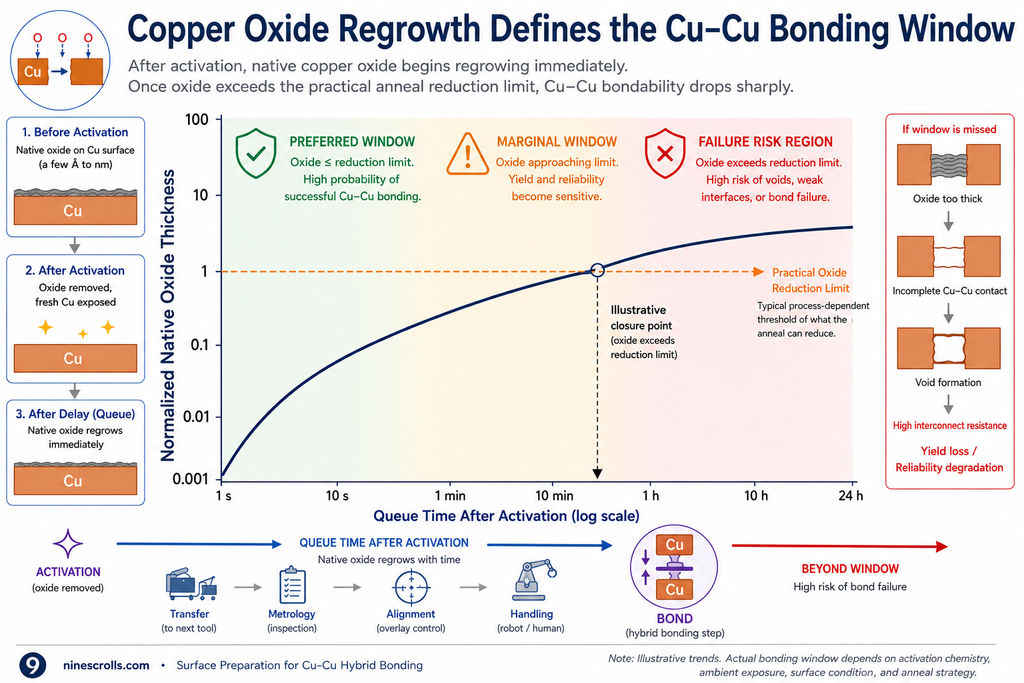
Because of this, queue time is controlled the way any critical parameter is. Fabs and labs set a maximum allowable queue time from activation to contact, route wafers automatically so they never stall at a hand-off, and minimize the air dwell at every transfer. The discipline is not optional polish; it is what keeps the copper inside the window the anneal can still close.
The mitigations follow directly from the kinetics. First, minimize air exposure between activation and contact — the shorter the dwell, the thinner the oxide. Second, bond under a reducing or forming-gas ambient: an N₂/H₂ atmosphere suppresses oxide growth and can reverse what little has formed, holding the copper bondable through the moments before contact. Third, store and transfer wafers under vacuum or inert N₂ rather than air, so the clock effectively pauses between steps. Together with tight, monitored queue-time limits, these keep the copper surface ready until the pads can interdiffuse on the post-bond anneal — the step the bonding hub takes from here.
One structural detail belongs to the copper as well: beneath each pad sits a diffusion barrier — TaN, TiN, or Ru, typically deposited by ALD — that keeps copper out of the surrounding dielectric through the thermal budget that follows. It sits below the surface the bond sees, but it is why the copper stays where it belongs.
7. Metrology and Inspection
Every link in the conditioning chain has a measurement that proves it, and the reason to run them all is that the bond is irreversible: once the wafers touch and the anneal fires, there is no rework. Surface prep you cannot verify is surface prep you cannot trust. So before a wafer is committed, each property the earlier sections demanded is checked against its spec, and only a surface that passes all of them is called ready.
Roughness — AFM. Atomic force microscopy resolves the sub-nanometer RMS finish the CMP step (§3) requires, confirming the dielectric is smooth enough to close.
Recess — profilometry, reflectometry, interferometry. The step height between recessed copper and the dielectric plane is measured directly, verifying the pads sit inside the narrow recess window §3 and §6 depend on — too deep and the joint opens, too shallow and a void forms.
Particles — laser-scattering inspection. A defect scan counts and sizes particles against the threshold §4 sets, since a single sub-micrometer particle nucleates a void far larger than itself.
Surface energy — water contact angle. A drop of water gives a fast proxy for the dielectric's surface energy after activation (§5): a low contact angle confirms the surface took the activation, while a contact angle drifting upward over a queue may indicate the activated surface is degrading before the wafer reaches the bonder.
The result — SAM and IR transmission. Scanning acoustic microscopy and infrared transmission image the post-bond interface for voids. This is the one measurement taken after contact, and it closes the loop: a void-free scan confirms that every upstream step — flatness, recess, cleanliness, activation, copper readiness — actually did its job.
The surface is only "ready" when roughness, recess, particles, and surface energy have each been verified in spec. A number missing from that set is a link in the chain taken on faith — and on a bond that cannot be reworked, faith is what the void scan later turns into yield loss.
8. Failure Modes Mapped to Surface Preparation
The conditioning chain is also a fault tree. Each defect that shows up at the interface points back to a specific link that was out of spec, and three of the four signature failures each belong to one step.
Non-contact void. The general void — two surfaces that failed to close — traces to whichever link left the surface unable to mate: CMP non-planarity or residual roughness (§3), incomplete cleaning (§4), or under-activation that left the dielectric energy too low (§5). It is the one defect with more than one possible parent, which is exactly why metrology checks all three.
Particle-induced void. This one is unambiguous: it owns post-CMP cleaning (§4). A single sub-micrometer particle props the wafers apart and opens a void hundreds of micrometers across — the disproportionate failure, and the reason cleaning is the largest yield lever after CMP.
Open or weak copper joint. The pads failed to interdiffuse. Either copper oxide grew past what the anneal can reduce — a queue-time overrun (§6) — or the recess was too deep for the copper to expand into contact (§3). The dielectric around it may have bonded perfectly; the metal is what failed.
Proud-copper void. The mirror image: too little recess, or copper left proud of the dielectric (§3), props the surfaces apart before they can mate and opens a void around each pad.
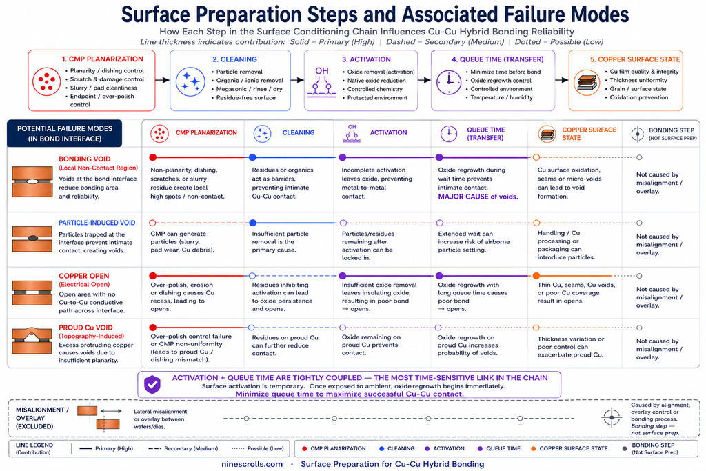
One failure deliberately does not appear on this map. Misalignment — overlay error that lands pads off-register and produces opens and shorts — is a real and serious hybrid-bonding failure, but it is not a surface-preparation defect. It originates at the bonding step: aligner overlay accuracy and wafer distortion at the moment of contact, neither of which any conditioning step touches. It is out of scope here by design; for the bonding step that owns it, see the Wafer Bonding Technologies Guide.
These surface-origin defects are where bond-yield loss begins. How each manifests in a finished stack — and how to read a void scan back to its root cause — is the failure-analysis side of hybrid bonding, a discipline we take up in a guide of its own.
Once the surface has been planarized, cleaned, activated, oxide-controlled, and verified, the bonding step itself becomes far more predictable. Everything that decides whether a hybrid bond takes has, by that point, already happened.
Frequently Asked Questions
What surface conditions does Cu-Cu hybrid bonding require?
Four, together: sub-nanometer dielectric roughness, coplanarity with the copper recessed a few nanometers, particle counts low enough that none nucleates a void, and a plasma-activated, oxide-free surface at contact.
Why is queue time critical before hybrid bonding?
Copper re-oxidizes in air within minutes. Queue time — the clock from activation to contact — is a hard spec: wait too long and the native oxide exceeds what the anneal can reduce, and the bond fails regardless of how good every earlier step was.
How is copper oxide removed before bonding?
Plasma activation reduces the native oxide; the harder problem is keeping it off until contact — via a reducing/forming-gas (N₂/H₂) ambient, inert storage, minimal air dwell, and tight queue-time limits (§6).
What roughness and dishing does CMP need to hit for hybrid bonding?
Rule of thumb: dielectric roughness below ~0.5 nm RMS, and copper recess held within a window often only a couple of nanometers wide, uniformly across the wafer (§3).
Why does plasma activation enable room-temperature dielectric bonding?
It raises the dielectric's surface energy by terminating it with reactive species, so two activated faces bond on contact at room temperature instead of needing a high-temperature step to initiate (§5).
How long can a wafer wait between activation and bonding?
The allowable queue time is process-specific and should be established experimentally for a given stack and ambient. In practice many flows operate on the order of tens of minutes to a couple of hours under controlled storage; beyond that window, re-oxidation closes the bond. Treat it as a monitored spec, not a convenience.
Surface preparation is the part of hybrid bonding most under your control — and the part that decides the most. NineScrolls builds the plasma equipment behind two of its links: our plasma cleaners for cleaning and dielectric activation, and our ICP-RIE systems for controlled, low-energy surface activation. If you are scoping a hybrid-bonding or 3D-integration surface-prep flow, we are glad to talk through where they fit.