Hybrid Bonding Failure Analysis: Detecting, Imaging, and Root-Causing Bond Defects
By NineScrolls Engineering · 2026-06-02 · 15 min read · Process Integration
Target Readers: Failure-analysis, packaging, and reliability engineers diagnosing Cu-Cu hybrid bonding defects in 3D-integrated devices, advanced memory, and CMOS image sensors.
This guide is about diagnosis — how a hybrid-bonding defect is detected, imaged, characterized, and traced to root cause. For what can go wrong at a high level, see our Wafer Bonding Technologies Guide; for how these defects originate in surface preparation and how to prevent them, see Surface Preparation for Cu-Cu Hybrid Bonding. This page picks up where prevention ends: you have a failing or suspect bond — now prove what happened.
1. The Failure-Analysis Mindset
Failure analysis begins with evidence, not defects. The engineer at the bench does not start by declaring "this is a void" or "this is copper oxide" — they start with a symptom (a die that fails electrical test, a stack that delaminates after thermal cycling) and work backward through evidence until the defect names itself. Naming the defect first is how diagnoses go wrong: it invites you to find the picture you expected instead of the one the part is showing you.
That distinction sets the boundary of this guide. The hub catalogues what can go wrong; Surface Preparation explains why defects originate and how to prevent them. This page answers a different question — how do I prove what happened? — and the answer is a disciplined chain from observed symptom to documented evidence to a defensible root cause. It is also the one place in the cluster where every defect type converges: void, particle, copper oxide, dishing, misalignment, and delamination all land on the same bench, because at the moment of observation the FA engineer does not yet know which one they have. The same symptom can point to different defect families, which is why it is the evidence — not the symptom — that owns the diagnosis.
2. The FA Workflow
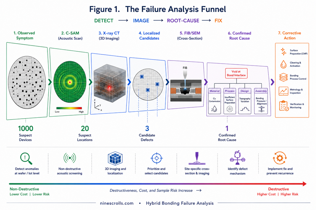
Hybrid-bonding failure analysis follows a fixed sequence, and the discipline is in not skipping forward. Each stage either localizes the problem or builds the evidence the next stage needs, and the most destructive techniques come last — once you cross-section a part, you cannot un-cut it.
- Observed symptom. An electrical failure, a yield excursion, a reliability reject — the entry point, no defect assumed.
- Non-destructive inspection. Acoustic, X-ray, and IR imaging find and locate anomalies without touching the part.
- Physical characterization. Cross-section, SEM, and TEM expose the interface and resolve morphology and chemistry.
- Evidence correlation. The electrical signature and the physical image are reconciled into one consistent story.
- Suspect root-cause family. The evidence points to a category — surface-state, particle, alignment — not yet a process knob.
- Corrective action. The suspect family hands off to the team that owns prevention.
The sections that follow walk this chain: first the defect signatures you are matching against (§3), then the inspection and physical-analysis toolboxes that produce the evidence (§4–§5), the electrical methods that localize it (§6), and finally how the evidence resolves to a suspect family (§7) — including defects that only surface under reliability stress (§8). Every tool in the toolbox that follows exists to move a failure one step further down this chain.
3. Failure Signatures & Evidence
This section is a defect-indexed lookup: match the symptom in front of you against a signature, confirm it with the listed evidence, and run the next technique. Each entry describes only what is observed at the bench — never how the defect got there. For where these defects come from and how to prevent them, see Surface Preparation.
Void (non-contact). Signature: a local open or high-resistance reading confined to one region. Evidence: a dark or echo indication in C-SAM, a low-density volume in CT, and a visible gap in cross-section. Next step: CT to map the extent, then cross-section through it.
Particle-induced void. Signature: a single isolated void disproportionately larger than any nearby feature. Evidence: a ring or halo in C-SAM, with cross-section showing a particle at the center. Next step: cross-section and SEM the void center to confirm the particle.
Copper open / oxide interface. Signature: elevated contact resistance or an open at the bond plane while the dielectric appears intact. Evidence: a thin interfacial layer at the Cu-Cu plane in TEM, with EELS or EDS showing oxygen localized at that plane. Next step: site-specific FIB plus TEM/EELS across a suspect pad.
Proud-copper void. Signature: localized non-contact around the pad perimeter — voiding that rings the copper pads rather than appearing in the dielectric field. Evidence: cross-section showing copper standing above the dielectric plane with a gap around it. Next step: cross-section across both pad and field to compare the two.
Misalignment / overlay. Signature: a daisy-chain resistance shift, with opens or shorts appearing at sites that should test good — the point where every defect family converges, since the symptom alone does not name it. Evidence: overlay metrology and a FIB cross-section showing pads off-register. Next step: overlay measurement, then a targeted cross-section at a suspect site.
Delamination. Signature: intermittent or stress-dependent opens, sometimes with audible or visible separation. Evidence: a large-area echo in C-SAM and an interface separation in cross-section. Next step: a C-SAM map to find the front, then cross-section at it.
When the defect is still unnamed, the symptom alone fixes the first tool to reach for — the Symptom-to-First-Tool Quick Reference below collapses the entries above into that single decision.
| Symptom | First tool |
|---|---|
| Open circuit | Electrical test |
| High resistance | Daisy chain |
| Void indication | C-SAM |
| Delamination | C-SAM |
| Misalignment suspicion | Overlay / cross-section |
| Interfacial anomaly | TEM |
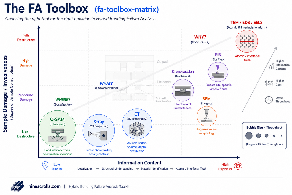
4. FA Toolbox I — Non-Destructive Inspection
Before any cut, the FA engineer reaches for tools that find and locate an anomaly without touching the part. Read this table down the technique column — the screening question is always coverage versus resolution.
| Technique | Detects | Typical Resolution | Throughput | Key Limitation |
|---|---|---|---|---|
| C-SAM (scanning acoustic microscopy) | Voids, delamination, unbonded area at the bond interface | ~µm-class lateral, interface-depth | High (full-wafer / full-area screening) | Needs acoustic coupling; limited on very thin or stacked layers; misses sub-resolution voids |
| 2D X-ray | Gross voids, bridging, large overlay error, foreign material | ~µm | High | Poor contrast for low-Z / thin interfacial features; planar projection hides depth |
| X-ray CT / 3D X-ray | 3D void distribution and location through the stack | Sub-µm to µm (sample-size dependent) | Medium–Low | Slow; small field of view at high resolution; sample size limited |
| IR (infrared) transmission / microscopy | Buried-interface anomalies, gross voids on IR-transparent stacks | ~µm | Medium | Only works through IR-transparent layers; blocked by metal or heavily doped Si |
The engineer sequences these by throughput: C-SAM first, because it screens a full wafer or area fast and flags where the interface is unbonded. X-ray and CT follow to localize the indication in three dimensions and resolve through the stack, trading speed for depth. IR is used where the stack is transparent enough to permit it. All of this happens before any destructive step — these techniques locate the anomaly so the cross-section, SEM, and TEM work in §5 is aimed at a known coordinate, not exploratory. The throughput column is the practical screening question at the bench: 100 dies in an afternoon, or one sample overnight.
5. FA Toolbox II — Physical Analysis
Physical analysis trades non-destructiveness for information: each step down this list destroys more of the part and reveals more of the interface.
| Technique | Reveals | Destructiveness |
|---|---|---|
| Mechanical polish / lapping | Exposes the bond interface in plan or angled view | Semi-destructive |
| Decapsulation | Removes mold/package to reach the die for package-level issues | Semi-destructive |
| Cross-section (mechanical / ion polish) | Interface morphology — voids, gaps, recess, separation | Destructive |
| FIB (focused ion beam) | Site-specific extraction of a single suspect pad / region | Destructive (localized) |
| SEM | Interface structure and void morphology at high magnification | Destructive (on a section) |
| TEM | Atomic-scale interface — the Cu-Cu bond plane, interfacial layers | Highly destructive |
| EDS / EELS | Interfacial chemistry / composition (e.g. oxygen at the bond plane) | Highly destructive (on a TEM lamella) |
This section embodies one trade-off. C-SAM (§4) is non-destructive but low-information; TEM/EELS is fully destructive but resolves the bond at atomic and chemical scale. The FA engineer climbs this ladder only as far as the question requires, and only after non-destructive inspection (§4) has aimed the cut — you spend the part once, so you spend it on a known coordinate. That least-destructive-to-most-destructive axis against information yield is exactly what Figure 2 plots. No single tool dominates the matrix; each occupies a different operating point, which is why a real FA flow uses several in sequence rather than one.
6. Electrical Failure Analysis
Hybrid bonds are not tested one pad at a time — they are tested through daisy chains and Kelvin / four-point test structures designed into the wafer. A daisy chain is a long series of bonded pads wired into one continuous loop, so a single resistance measurement reports on hundreds or thousands of interfaces at once; a Kelvin structure isolates the resistance of an individual contact by separating the force and sense paths. These structures exist because chain resistance is the earliest, cheapest signal that an interface is marginal — you read a number before you cut anything.
A resistance excursion — a chain that reads high against its reference, or an outright open — is usually the first evidence of a bonding problem, well before any imaging. A clean Cu-Cu interface adds negligible series resistance; an oxidized or incompletely bonded one does not, and a missing contact reads as infinite. The chain tells you that something is wrong long before C-SAM or cross-section tells you what it is.
What it does not tell you, by itself, is where. Failure isolation is the work of narrowing a chain-level failure to a specific region or a specific pad. Chain-segment resistance brackets the failing site between voltage taps; Kelvin taps measure individual contacts directly; and active techniques — OBIRCH, thermal-emission microscopy, EOTPR (time-domain reflectometry) — localize where the open or high-resistance site sits along the chain. The point of all of this is economy of destruction: it lets the cross-section, FIB, and TEM work of §5 be aimed at one coordinate instead of an entire die.
This is the leverage of electrical FA. It tells you where before physical FA tells you what — it converts "this die fails" into "this pad, this chain segment," and that conversion is what makes the rest of the analysis affordable.
Correlating Electrical and Physical Evidence
Electrical FA tells you where to cut; physical FA tells you what the cut reveals. The full chain runs in one direction: a high-resistance or open daisy-chain reading flags the failure, failure isolation narrows it to a region or pad, CT localizes the suspect site in three dimensions through the stack, and a cross-section or TEM lamella is taken at that exact site. Electrical FA and physical FA are not two separate workflows that happen to share a part — the electrical result aims the physical cut, and the physical image then confirms or overturns the electrical hypothesis. A chain that reads open and a cross-section that shows a clean separated interface at the isolated pad are the same finding, observed twice.
This correlation layer is what separates rigorous failure analysis from "image something and hope." Without it, you cut blind and report whatever the section happens to show; with it, every destructive step is a test of a prior electrical hypothesis, and a result that contradicts the electrical signature is a signal to keep looking rather than a defect to write up. The discipline stops here at the physical evidence — naming the process that produced it belongs to §7.
7. Root-Cause Decision Tree
The FA engineer's job ends at a defensible suspect family — the category the correlated evidence implicates — and hands off there to the team that owns prevention. The tree below maps evidence to a suspect family to where the investigation continues; it deliberately stops short of naming the process that produced the defect.
- C-SAM void + clean dielectric in cross-section → suspect a surface-readiness issue (planarity / cleanliness) → see Surface Preparation.
- Isolated void with a particle at its center in cross-section → suspect a particle / contamination issue → see Surface Preparation.
- TEM interfacial layer + EELS oxygen at the bond plane → suspect a copper-surface-state issue → see Surface Preparation.
- Daisy-chain resistance shift + overlay error on cross-section → suspect a bonding-step alignment issue → see Wafer Bonding Technologies Guide.
- Large-area C-SAM echo appearing only after stress → suspect a marginal / latent interface → reliability evolution, §8 below.
Read the tree by evidence, not by process step: the left column is what you observed at the bench, the right column is the family that owns it and where the trail continues. The same discipline that aimed every cut now constrains the conclusion — you report the suspect family the evidence supports, no further.
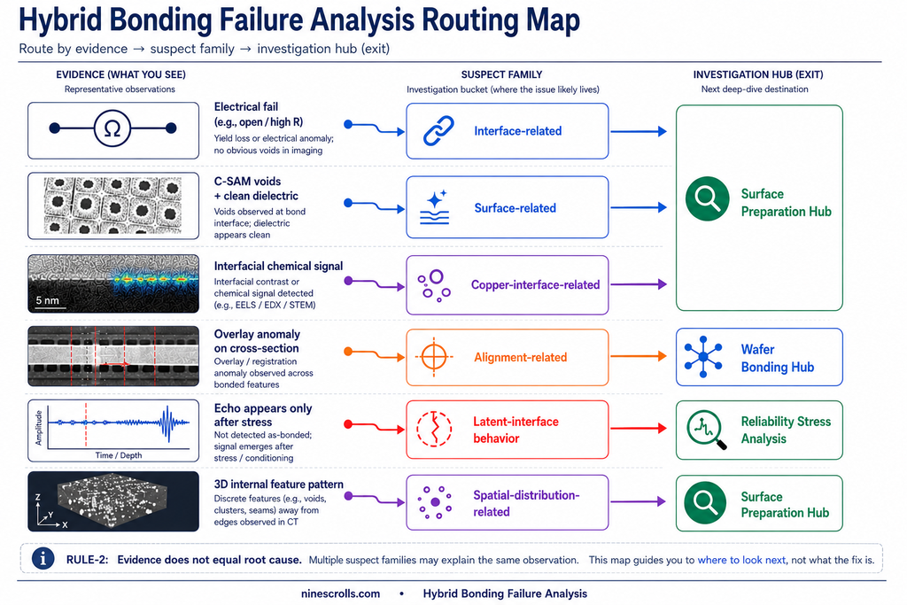
Reading the Tree
A single piece of evidence rarely fixes a family on its own — the tree is read by convergence, not by first hit. A C-SAM void could be a planarity problem or a particle; only when the cross-section shows a clean interface with no particle at the center does the surface-readiness family hold. A daisy-chain open could be misalignment or a copper-oxide joint; overlay metrology and a TEM interfacial check separate the two. The rule is to require two independent observations — typically one electrical or non-destructive, one physical — to point at the same family before you assign it. A lone indication is a lead, not a conclusion, and assigning a family on one ambiguous signal is how an FA report sends the wrong team chasing the wrong fix.
That is the boundary of this guide: the chain ends at a suspect family, and the named process cause together with its correction lives in the linked guides, not here.
8. Failure Evolution Under Reliability Stress
Reliability stress does not create defects — it reveals latent ones. A marginal interface that passed at t=0, that read clean on the chain and showed no echo in C-SAM, is not a good bond; it is a bad bond that has not yet failed. Stress is what advances it from passing to failing. For the underlying failure mechanisms — why these signatures arise in the first place — see Reliability Challenges in High-Density 3D Packaging. And once it fails, the FA workflow is the same one §2 through §7 already describe: the engineer does not care whether the part surfaced at bonding, at thermal-cycle read-point 500, or at HTOL 1000h — only what the evidence shows. The bench does not have a separate door for reliability rejects.
Thermal cycling (TC). Repeated thermal-expansion mismatch drives interfacial crack growth and propagates delamination outward from an already-marginal bond. FA signature: a C-SAM echo area that grows between read-points, and a cross-section showing a crack tracking along the interface from an existing front.
Electromigration (EM). Sustained current stress drives copper depletion and void nucleation at the Cu-Cu joint over time. FA signature: chain resistance that rises as the stress accumulates, with cross-section and SEM resolving voids at the bonded interface that were not present at t=0.
Temperature-humidity bias (THB). Moisture under bias degrades the dielectric and attacks the bond periphery. FA signature: degradation that works edge-in, corrosion products and leakage, with the physical analysis aimed at the die edge and seal rather than the field.
Because the workflow is time-agnostic, a reliability reject and a day-0 yield reject route to the same bench and run through the same suspect-family logic of §7 — the read-point that produced the part is metadata, not a different diagnosis.
Frequently Asked Questions
How do you detect voids in a hybrid bond?
Scanning acoustic microscopy (C-SAM) is the first tool — it images unbonded area at the interface non-destructively and screens at high throughput. X-ray CT then maps a void's 3D extent, and a cross-section confirms it. A local open or high-resistance reading is the electrical signature that sends you to C-SAM in the first place.
How is a copper-oxide bond defect confirmed?
By TEM on a site-specific FIB lamella across a suspect pad: an oxide interface shows as a thin interfacial layer at the Cu-Cu plane, and EELS or EDS confirms oxygen localized there. The electrical signature that points you to it is elevated contact resistance or an open while the surrounding dielectric appears bonded.
What is the difference between C-SAM and X-ray for hybrid bond inspection?
C-SAM uses ultrasound and is sensitive to unbonded interfaces — voids and delamination — making it the workhorse for bond-integrity screening. X-ray is sensitive to density and is better for gross defects, bridging, and foreign material; CT extends it to 3D localization. In practice C-SAM screens, X-ray/CT localizes.
How do you tell a surface-prep defect from a misalignment defect?
By the evidence, not the symptom — both can present as an open. A cross-section showing pads off-register points to a bonding-step alignment issue; a void or interfacial layer with pads correctly registered points to a surface-readiness issue. The root-cause tree (§7) routes the two to different owners.
What failure-analysis techniques are destructive vs non-destructive?
Non-destructive: C-SAM, X-ray, CT, and IR — they locate anomalies without touching the part. Destructive: cross-section, FIB, SEM, TEM, and EDS/EELS — they expose and resolve the interface but consume the sample. The discipline is to run the non-destructive tools first so the destructive cut is aimed.
How does reliability stress reveal latent bonding defects?
A marginal interface can pass at t=0 and fail later: thermal cycling propagates interfacial cracks and delamination, electromigration nucleates voids at the Cu-Cu joint, and temperature-humidity bias degrades the bond periphery. The failure surfaces at TC500 or HTOL 1000h, but the FA workflow that diagnoses it is the same one used at bonding.
Most hybrid-bonding root causes lead back to surface preparation — the part of the flow most under your control. NineScrolls builds the plasma equipment behind two of its links: our plasma cleaners for cleaning and dielectric activation, and our ICP-RIE systems for controlled, low-energy surface activation. If you are closing the loop from failure analysis back to prevention, we are glad to help.