Wafer Bonding Technologies for 3D Integration: From Fusion Bonding to Hybrid Bonding
By NineScrolls Engineering · 2026-06-01 · 25 min read · Process Integration
Target Readers: Process and packaging engineers, PIs and lab managers, and R&D teams evaluating wafer-bonding and advanced-packaging capability. Newcomers get the method map and the evolution arc; experienced engineers can jump straight to the hybrid bonding process flow, failure modes, and equipment requirements.
1. Why Wafer Bonding Matters
For most of the history of semiconductor manufacturing, "the chip" meant a single piece of silicon: transistors patterned on one wafer, wired together in metal layers stacked on top. Performance came from making those transistors smaller. That era is ending. Transistor scaling has slowed, the cost per transistor has stopped falling, and the industry has shifted its center of gravity from shrinking the device to integrating more devices together — vertically, in three dimensions. Almost every one of those 3D integration schemes ultimately rests on the same physical operation: taking two finished surfaces and joining them into one mechanically sound, electrically functional stack. That operation is wafer bonding.
The applications driving this shift are not niche. They are the highest-volume, highest-value products in the industry:
- HBM memory. High-Bandwidth Memory stacks 8, 12, and now 16 DRAM dies vertically, connected by through-silicon vias. Most leading AI accelerators depend on HBM-class stacked memory, and the move to 16-Hi stacking is pushing the industry toward finer-pitch interconnects, including hybrid bonding roadmaps. See our HBM4 & Advanced Packaging guide for the industry and thermal context.
- Chiplets and 3D logic. Rather than build one enormous monolithic die, designers now partition a system into smaller chiplets and stack or tile them on an interposer. Logic-on-logic stacking — placing cache or a second compute die directly on top of a processor — is bonded face-to-face at the wafer or die level.
- CMOS image sensors (CIS). Modern image sensors are two wafers bonded together: a photodiode array on top, the readout and logic circuitry underneath, connected pixel-for-pixel. This is one of the highest-volume hybrid bonding applications in production today.
- Silicon photonics. Integrating III-V laser material onto a silicon photonic circuit requires bonding dissimilar materials that cannot be grown on the same substrate. Heterogeneous integration of this kind lives or dies on bond quality.
- MEMS. Accelerometers, gyroscopes, pressure sensors, and microfluidic devices use bonding to seal cavities, cap fragile mechanical structures, and stack functional wafers. Our MEMS Fabrication Process Guide covers where bonding sits in that flow.
What unites these applications is a single requirement: two surfaces must be joined so that the interface is mechanically strong, hermetic where needed, electrically conductive where needed, and free of voids — often across an entire 300 mm wafer, and increasingly at interconnect pitches measured in micrometers or below. The rest of this guide maps the major bonding technologies, traces why the industry is converging on hybrid bonding, and walks through the process, failure modes, and equipment that determine whether a bond yields.
2. The Evolution of Wafer Bonding
Wafer bonding is not new. What has changed is which method sits at the center of the industry's attention — and the trajectory tells you where the engineering challenges have moved.
The earliest production methods joined wafers thermally or chemically. Fusion (direct) bonding brings two clean, flat surfaces into contact and anneals them until covalent bonds form across the interface — the foundation of silicon-on-insulator substrates. Anodic bonding joins silicon to glass under voltage and heat, long the workhorse for sealing MEMS cavities. Both prioritize a strong, hermetic seal; neither was designed to carry dense electrical interconnect across the bond.
As devices began to stack and communicate vertically, the requirement changed from "seal two wafers" to "seal two wafers and route thousands of electrical connections across the interface." Eutectic and adhesive bonding addressed specific material and process-compatibility needs along the way, but the decisive step toward electrical 3D integration was thermocompression bonding — joining copper-to-copper under heat and force, which made the bond itself an electrical conductor. Thermocompression, in turn, ran into a wall as interconnect density climbed, and that wall is precisely what hybrid bonding was invented to break through.
The arc, then, runs Fusion → Anodic → Eutectic → Thermocompression → Hybrid — from "join two surfaces" toward "join two surfaces with the highest possible density of electrical connections and the lowest possible profile." The next two sections map those methods in detail and then explain why the last step in that sequence has become the industry's defining packaging technology.
3. Major Wafer Bonding Technologies
Six bonding families cover essentially all production and advanced R&D today. They differ in what holds the interface together — covalent bonds, electrostatic force, a polymer, a metal alloy, or diffused metal — and that mechanism dictates temperature, surface requirements, and whether the bond carries current. The matrix below places them side by side; the subsections add detail.
| Method | Bonding temp | Materials | Bond strength / character | Typical use |
|---|---|---|---|---|
| Fusion (direct) | RT contact + anneal; 1000–1100 °C classic, <400 °C plasma-activated | Si–Si, Si–SiO₂, oxide–oxide | Covalent; very strong, hermetic; insulating interface | SOI, sensor stacking, MEMS |
| Anodic | 300–450 °C + 200–1000 V | Si–borosilicate glass (Pyrex/Borofloat) | Electrostatic + chemical; strong, hermetic; insulating | MEMS cavity sealing, microfluidics |
| Adhesive | 150–250 °C | BCB, polyimide, SU-8 on most substrates | Polymer; moderate, not hermetic; topography-tolerant | Temporary bonding, heterogeneous integration |
| Eutectic | Au–Sn ~280 °C; Al–Ge ~430 °C; Cu–Sn ~280 °C | Patterned metal layers on both wafers | Eutectic alloy; strong, hermetic; conductive | MEMS caps, optoelectronic packaging |
| Thermocompression (Cu–Cu) | ~300–400 °C + applied force | Cu pads/pillars, oxide-free | Metallic diffusion; strong; electrically conductive | 3D logic, microbump-pitch interconnect |
| Hybrid | RT contact + 150–300 °C anneal | Cu pads inlaid in dielectric (SiO₂/SiCN) | Simultaneous dielectric + Cu–Cu bond; no bump | CIS, HBM, fine-pitch 3D stacking |
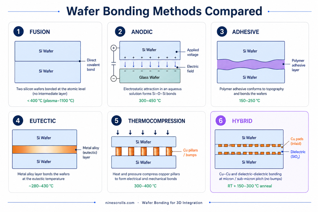
Fusion (Direct) Bonding
Fusion bonding joins two surfaces with no intermediate layer — the wafers themselves become the bond. The price is surface preparation: the mating faces must hold roughness below roughly 0.5 nm RMS and tight flatness, since particles or waviness invisible elsewhere open voids here. Contacted at room temperature, the surfaces adhere through van der Waals forces into a weak pre-bond that annealing converts to full covalent strength. The classic anneal runs at 1000–1100 °C; plasma activation beforehand develops the same strength below 400 °C, making it compatible with temperature-sensitive devices. It is the foundation of silicon-on-insulator substrates and a workhorse for MEMS wafer stacking.
Anodic Bonding
Anodic bonding joins silicon to a borosilicate glass — typically Pyrex or Borofloat, whose thermal expansion is matched to silicon so the stack does not crack on cooling. With the wafers heated to 300–450 °C and 200–1000 V applied (glass negative), mobile sodium ions migrate from the interface, leaving a depletion layer whose space charge pulls the surfaces together while oxygen forms permanent Si–O bonds. That strong, hermetic seal made anodic bonding the standard for sealing the cavities of pressure sensors, accelerometers, and other MEMS devices and capping microfluidic channels. It needs a glass partner and an applied field, and the interface is insulating — it seals but does not interconnect.
Adhesive Bonding
Adhesive bonding uses an intermediate polymer — benzocyclobutene (BCB), polyimide, or SU-8 — spun on, contacted, and cured at 150–250 °C. Because the polymer flows before it sets, it conforms to fill gaps, tolerating surface topography, residual particles, and mismatched materials. That makes it the natural choice for temporary bonding — a device wafer held to a carrier through thinning, then released — and heterogeneous integration. For the carrier system and how to remove it, see Temporary Wafer Bonding and Debonding. The trade-off is the polymer itself: the bond is not hermetic, and its thermal and mechanical stability falls short of any inorganic method.
Eutectic Bonding
Eutectic bonding forms a metallic alloy at the interface. Patterned metal layers — gold–tin, aluminum–germanium, or copper–tin — are heated past their eutectic (Au–Sn and Cu–Sn near 280 °C, Al–Ge near 430 °C), where a liquid alloy forms, wets both surfaces, and solidifies into a continuous bond that fills small gaps. The joint is strong, hermetic, and conductive, making it a mainstay for MEMS caps that seal a cavity at controlled pressure and for optoelectronic packaging where it doubles as an electrical and thermal path. The cost is the patterned metal deposition both wafers require.
Thermocompression Bonding (Cu–Cu)
Thermocompression bonding (TCB) is the method that first made the bond itself the electrical connection. Copper pads or pillars on the two wafers are aligned and pressed together under simultaneous heat and force — typically 300–400 °C with substantial pressure — until copper diffuses across the interface and the pads merge into one continuous metal. With no solder and no intermediate alloy, the joint conducts as well as the surrounding metal.
The central difficulty is the copper surface: even a few nanometers of native oxide block diffusion and starve the bond, so the surfaces must be kept oxide-free up to contact, often under a forming-gas or formic-acid treatment. Diffusion across a non-planar surface then demands high force and temperature held for a long dwell — the force must reach every bond at once, the thermal budget is significant, and the long cycle throttles throughput. Built around discrete copper pads, TCB does not scale to the densities the next generation wants.
These limits matter because thermocompression is the direct technical ancestor of hybrid bonding, which keeps the copper-to-copper diffusion TCB pioneered but rethinks everything around it to escape them.
Hybrid Bonding
Hybrid bonding is the method this guide builds toward, so it is worth defining precisely. In a hybrid bond, each wafer presents a single planarized surface in which copper pads are inlaid flush within a dielectric — usually silicon oxide or silicon carbonitride (SiCN). The surface is, in effect, a damascene field of metal islands set in insulator, polished by chemical-mechanical planarization until the copper and the dielectric sit in the same plane to within a few nanometers. There is no bump, no pillar, and no solder standing above the surface; the entire mating face is flat.
The bond forms in two stages, and this is what makes it "hybrid" — two bond types created in one joint. First, the dielectric surfaces are plasma-activated and brought into contact at room temperature, where they bond to each other immediately, much as in fusion bonding: a dielectric-to-dielectric bond closes the interface and holds the wafers together with no applied force. Then the pair is annealed at a modest 150–300 °C. During the anneal the copper, which has a higher thermal expansion than the surrounding dielectric, expands and the recessed pads grow into contact across the interface, where they diffuse and merge into copper-to-copper bonds — the same diffusion mechanism as thermocompression, but driven by controlled expansion rather than brute external force. The outcome is a single interface that is simultaneously a dielectric seal and a dense array of electrical connections.
This flat, bumpless interface is what lets hybrid bonding move past the scaling limits that constrain every bump-based method. It is also unforgiving — the planarization, cleanliness, and alignment demands are severe, and much of the rest of this guide is about them. Why this particular method came to dominate advanced packaging, and why the industry is willing to absorb its process complexity to get it, is the subject of the next section.
4. Why Hybrid Bonding Became the Industry Focus
The previous section can read like a menu: six bonding families, hybrid bonding simply the newest. That misses what is happening. Hybrid bonding is not one option among equals — it is the endpoint the evolution arc of §2 was converging on. The industry adopted it not because it was novel but because the path from fusion through thermocompression had nowhere left to go, and hybrid bonding was the only method that removed the obstacle blocking the next decade of integration. Understanding why means following one chain of consequences, each link forced by the one before, starting with a number.
That number is interconnect pitch — the center-to-center spacing of the connections crossing the bond. Every bump-based scheme, thermocompression included, places solder or a copper pillar between the dies. Solder sets a floor on pitch: the volume needed for a reliable joint bridges to its neighbor if the spacing shrinks too far, and the inter-die gap needs underfill, which needs room to flow. In production this drives microbump pitch to a practical wall near 20–40 µm. Aggressive development has pushed solder toward ~10 µm, but only at steep cost in yield and throughput — the wall bends, it does not move. Hybrid bonding removes the bump. With copper inlaid flush in dielectric, there is no solder to bridge and no underfill gap, so pitch is set not by metallurgy but by lithography and overlay accuracy. Demonstrated hybrid-bond pitches are already well below 10 µm, with production image sensors in the low single-digit micrometer range and roadmaps targeting ~1 µm and below.
Translate that into area density and the magnitude shows. Density scales as the inverse square of pitch: moving from 40 µm to 1 µm is a 40× reduction in spacing and roughly 1,600× more connections per unit area; even a conservative 20 µm-to-2 µm comparison gives about 100×. A microbump array tops out near a few hundred to a couple thousand connections per square millimeter; a hybrid interface at single-micrometer pitch carries hundreds of thousands. That is two to three orders of magnitude — the difference between routing a bus across the interface and routing an on-chip metal layer across it.
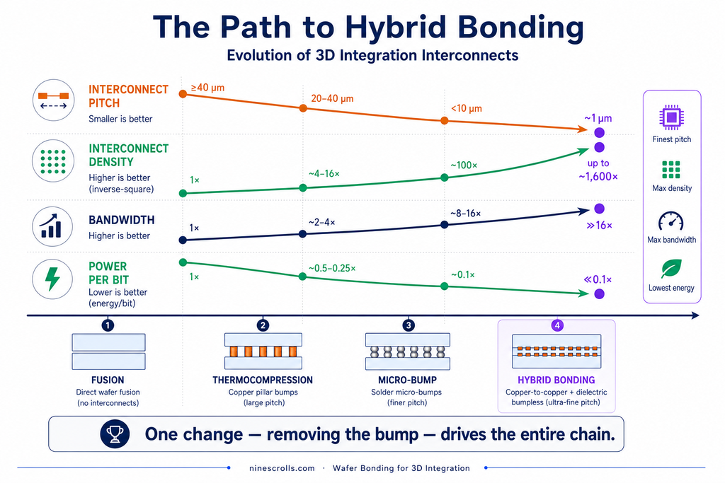
Density is not the goal; it is the means to bandwidth, the link the market actually pays for. Aggregate bandwidth is the number of parallel connections times the rate each carries. Per-link rate is capped by signaling physics, so once it is maxed the only lever left is more links in parallel — exactly what density buys. An interface with two to three orders of magnitude more connections in the same area delivers a corresponding leap in total bandwidth with no increase in any link's clock. This is the mechanism behind the memory bandwidth modern AI accelerators rely on, and behind logic-on-logic stacking, where a cache or compute die must reach the processor beneath it at on-die rather than package bandwidths. For the HBM-specific structural picture and the constraints of tall stacks, see our HBM4 & Advanced Packaging guide.
Bandwidth is inseparable from power, and this is the link that turns advantage into necessity. The energy to move a bit is paid against the path's parasitic capacitance and resistance. A solder bump with its underfill gap is a long, high-capacitance structure; a hybrid bond is a short copper-to-copper junction flush in the surface, with a fraction of the parasitic load — lower capacitance, less energy per bit. In a leading-edge AI accelerator, data movement, not computation, dominates the power budget, and the energy of shuttling data between memory and logic limits what the system can do in a fixed thermal envelope. Cutting energy per bit at the busiest interface is not a refinement; it is what makes the next generation thermally feasible.
The last link is signal integrity and latency, from the same geometry. A shorter path carries less inductance and resistance, and removing the bump eliminates the inductive discontinuity a tall solder joint adds to a high-speed link. Tighter coupling and lower parasitics give cleaner signaling and lower latency. The one bumpless change that raised density, bandwidth, and efficiency improves every signal crossing the bond as well.
A profile and thermal dividend rides alongside. With no bump or underfill, each interface adds far less height — decisive in a twelve- or sixteen-die HBM stack where every micrometer compounds and heat extraction is already the binding constraint — and the direct copper path eases heat out of the stack. We keep this secondary: the spotlight belongs on the density-to-bandwidth-to-power chain, which is what made hybrid bonding inevitable rather than merely attractive.
None of it is free, and the industry's willingness to pay is the measure of the payoff. The flat, bumpless interface demands surfaces flatter and cleaner than any other method needs: CMP holding copper and dielectric coplanar to a few nanometers, sub-nanometer roughness, particle control where one sub-micrometer particle opens a void across thousands of connections, and plasma activation to start the dielectric bond. These exacting requirements are why hybrid bonding took years to reach volume. The industry paid anyway, because the chain above — from a 20–40 µm pitch wall down to sub-micrometer connections — is not a feature set hybrid bonding happens to offer; it is the only known way past the limit every bump-based method hits. For when to choose hybrid bonding over micro-bumps — the pitch zones, yield economics, and cost crossover — see Hybrid Bonding vs Micro-Bump: Where Each Technology Wins. How the process achieves those surface conditions, where it fails, and what equipment it takes are the subjects that follow.
5. The Hybrid Bonding Process Flow
This section walks through how the flat, bumpless interface is built. Each wafer arrives as a damascene field of copper pads inlaid in dielectric — silicon oxide or SiCN, the copper lined by a thin diffusion barrier deposited by ALD to keep it out of the insulator. Six operations turn two such wafers into one stack, and the order matters: each step prepares the surface for the next, and a defect introduced early survives every step after.
- CMP (chemical-mechanical planarization). An abrasive slurry against a polishing pad removes dielectric and copper together until both sit in one near-atomically-flat plane, tuned so the softer copper dishes a few nanometers below the dielectric by design — the recess that later lets the dielectric touch first and the copper close the gap on heating. The flatness CMP leaves sets the ceiling on everything downstream; no later step recovers a wavy surface.
- Cleaning. CMP leaves slurry residue and loose particles, and on a hybrid bond a single particle is catastrophically out of proportion to its size: it props the wafers apart and opens a void far larger than itself, swallowing many connections at once. A megasonic wet clean strips residue and particulates down to the level the bond demands; see our guide to plasma cleaner applications for related dry-cleaning approaches.
- Plasma activation. This is the step that decides bond quality. A low-energy plasma — N₂, O₂, or H₂ — does two things at once: it terminates the dielectric (SiO₂ or SiCN) with reactive species, raising its surface energy so dielectric-to-dielectric bonds form on contact at room temperature; and it strips native oxide from the recessed copper, leaving the metal ready to diffuse once heat is applied. The activated surface stores the energy that later drives the bond across the wafer — an under-activated or contaminated surface will not close. Our guide to plasma surface modification covers the mechanisms in depth.
- Alignment. The two activated wafers are positioned so every copper pad lands on its mate — pad-for-pad, across the whole wafer. At sub-micrometer pitch this is brutal: the overlay budget is a fraction of a pad width, and a pad that lands off its partner is an open or a short, not a weak joint. Alignment is fixed before contact, because once the surfaces touch they cannot be slid.
- Contact. The aligned wafers are touched at a single point, and a bond wave propagates spontaneously across the wafer at room temperature, the activated dielectric surfaces zipping together with no applied force — the surface energy from activation is what pulls the interface closed. The dielectric is now bonded, but the recessed copper pads are not yet connected.
- Annealing. The bonded pair is heated to a modest 150–300 °C. Copper expands far more than the dielectric, so the recessed pads grow outward, close the gap CMP left, and interdiffuse into continuous copper-to-copper bonds — the built-in dishing is exactly what this expansion takes up. The anneal completes the electrical connection and locks the dielectric bond in at full strength.
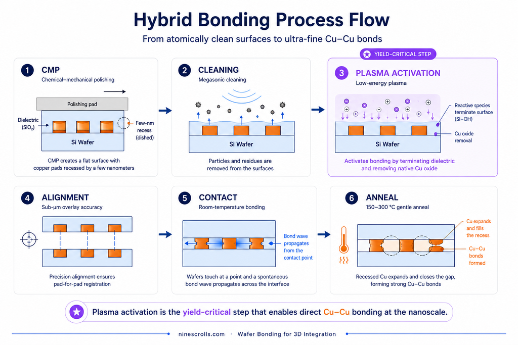
Read end to end, the flow is one chain of dependencies: CMP sets the plane and the dishing, cleaning protects it, plasma activation arms the dielectric and clears the copper, alignment registers the pads, contact closes the insulator, and the anneal closes the metal. Where any one step falls short is exactly where the next section's failure modes originate. The surface-conditioning half of this flow — CMP, cleaning, and plasma activation, plus copper-oxide queue-time control — is where bond yield is won or lost; our Surface Preparation for Cu-Cu Hybrid Bonding guide treats those steps in depth.
6. Failure Modes and Yield Challenges
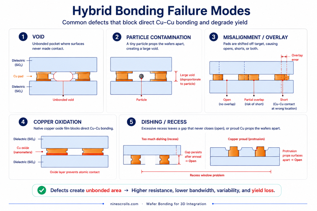
A hybrid bond fails at the interface, almost always because a condition the process flow worked to establish was not met. Five failure modes account for nearly all yield loss in production. For each: what the defect is, what causes it, and how the process holds it in check.
Voids
Mechanism. A void is an unbonded pocket where the two surfaces never made contact. Root cause. Trapped gas or adsorbed moisture, outgassing during anneal, non-planarity or waviness left by CMP, and incomplete bond-wave propagation all leave the interface locally open; voids are imaged after bonding by scanning acoustic microscopy (SAM) or infrared transmission. Mitigation. Tighter planarization and roughness control, pre-bond degassing, and an optimized activation and anneal ramp that lets trapped species escape rather than nucleate a pocket.
Particle Contamination
Mechanism. A single particle props the wafers apart locally and opens a void far larger than itself — a 1 µm particle can nucleate a void hundreds of micrometers across, swallowing many connections. Root cause. Residue left after CMP, or particles from handling and the bonding chamber. This is the single largest yield killer in hybrid bonding: the defect's footprint is orders of magnitude larger than its source. Mitigation. Rigorous post-CMP megasonic cleaning, low-particle handling, and a controlled chamber environment — disciplined plasma cleaner maintenance helps hold particle counts where the bond demands.
Misalignment / Overlay Error
Mechanism. At low-micrometer pad pitch, wafer-to-wafer overlay error shifts each pad off its mate — raised contact resistance where pads partially overlap, opens or shorts where they miss. Root cause. Limited alignment accuracy compounded by wafer distortion and run-out, which displace pads non-uniformly. Mitigation. High-accuracy alignment, distortion compensation, and the die-level versus wafer-level trade where smaller registered areas relax the overlay budget.
Copper Oxidation
Mechanism. Native oxide on the recessed copper blocks the Cu-Cu interdiffusion the anneal must drive, giving weak or open joints even where the dielectric bonded cleanly. Root cause. Copper oxidizes in air within minutes, so any delay between activation and bonding lets oxide regrow — a time-sensitive, queue-dependent defect. Mitigation. Minimizing air exposure, bonding under a reducing or forming-gas ambient, and tight activation-to-bond queue-time control.
Copper Dishing / Recess
Mechanism. CMP leaves the copper recessed by design so the dielectric bonds first and the copper expands on anneal to close the gap. The defect is a recess outside its window: too much leaves a gap the copper cannot close (an open); too little leaves the copper proud, propping the dielectric apart (voids). Root cause. CMP recipe drift in the relative removal rate of copper and dielectric. Mitigation. Recipe tuning to hold the recess in a tight window, with recess metrology measuring the copper-to-dielectric step every lot.
These five modes are not independent — most trace back to a surface condition set upstream, which is why control discipline at CMP, cleaning, and activation governs yield more than anything done at the bonder itself. For how each of these defects maps back to the specific surface-preparation step that causes it, see Surface Preparation for Cu-Cu Hybrid Bonding. For how to detect, image, and root-cause those defects once a part has failed, see Hybrid Bonding Failure Analysis.
7. Equipment Required Across the Bonding Workflow
Each step in the flow places a hard specification on the tool that runs it, and a shortfall against that spec does not produce a marginally worse bond — it surfaces directly as one of the failure modes above. What follows is not what the equipment does, but what it must deliver to keep yield intact.
CMP must hold the wafer planar to within a few nanometers of global non-uniformity and leave sub-nanometer post-polish roughness, while keeping copper recess inside a window often only a couple of nanometers wide across the full wafer. Planarity and roughness shortfalls become the voids of §6; recess that drifts off target becomes the dishing-induced opens and proud-copper voids. The tool's defensible spec is removal-rate uniformity and copper-to-dielectric selectivity that hold lot to lot, not just on a center die.
Cleaning must strip slurry residue and sub-micrometer particulates to the bond's threshold without re-depositing what it removes — re-deposition is itself the particle-contamination mode, where a single 1 µm particle nucleates a void hundreds of micrometers across. The capability that matters is particle removal efficiency at the relevant size with verified non-redeposition.
Plasma activation is the single most critical yield driver in the entire flow: it must deliver uniform radical exposure across the full wafer at controlled, low ion energy, because non-uniform activation leaves under-energized regions that simply will not close, and excess ion energy roughens the surface it is meant to prepare. This is where surface preparation either earns or forfeits the bond — and it is the capability NineScrolls builds equipment around. Our ICP-RIE systems deliver the controlled low-energy plasma surface prep this step needs, and our plasma cleaners handle the cleaning and activation that protect it; the RIE guide and Plasma Cleaner Buying Guide go deeper on selection. The barrier and dielectric layers underneath come from ALD systems, with coater/developer capability covering the litho-adjacent prep.
Alignment and metrology must register the wafers to sub-micrometer overlay accuracy and compensate for in-plane wafer distortion and run-out, since uncompensated distortion displaces pads non-uniformly and produces the overlay opens and shorts of §6. The companion requirement is inspection: SAM and infrared imaging capable of resolving voids and overlay error after bonding, because a defect that escapes detection ships.
The bonding tool must provide a particle-controlled chamber environment and deliver force and temperature uniformly across the whole wafer — local force or thermal gradients translate into uneven contact and incomplete bond-wave propagation. The anneal, finally, must apply a uniform thermal budget across the stack, since a thermal gradient leaves some copper joints under-diffused while others over-expand. Across the flow, the equipment specification is the yield specification.
8. Future Directions
The trajectory is already set: every interface that needs density is moving onto copper-to-copper hybrid bonding. HBM4E and HBM5 push the stack taller and the die-to-die pitch finer, displacing the last solder microbumps from the memory cube. Logic-on-logic stacking — cache and compute partitioned across face-to-face bonded chiplets — extends the same physics into the processor itself, and chiplet architectures make wafer-to-wafer and die-to-wafer hybrid bonding a default assembly step rather than an exotic one. For when to choose which format, see Wafer-to-Wafer vs Die-to-Wafer. Silicon photonics remains the outlier, bonding III-V laser material onto silicon where heterogeneous integration still leans on adhesive and direct bonds alongside hybrid. The table below maps where each application is heading.
| Application | Dominant bonding trend |
|---|---|
| HBM memory | Hybrid (Cu-Cu) |
| Logic-on-logic | Hybrid (Cu-Cu) |
| CMOS image sensors (CIS) | Hybrid (Cu-Cu) |
| Silicon photonics | Hybrid + adhesive (heterogeneous III-V/Si) |
| MEMS | Fusion + anodic |
None of this stands alone. Hybrid bonding and TSV technology are increasingly co-optimized in modern 3D integration schemes, since the vias that carry signal through a thinned die and the bonded interface that joins dies are now designed as one electrical path. For the via half of that path — integration timing and design rules — see Through-Silicon Vias (TSV). For the HBM-specific roadmap and the thermal and materials constraints that come with taller stacks, see our HBM4 & Advanced Packaging guide.
Frequently Asked Questions
What is wafer bonding?
Wafer bonding is the process of joining two wafers into a single stack — mechanically, hermetically, and where needed electrically. It is the foundational operation behind 3D integration, turning separately fabricated wafers into one functional assembly.
What is hybrid bonding?
Hybrid bonding forms a dielectric-to-dielectric bond and a copper-to-copper bond simultaneously on a single planarized surface. With copper inlaid flush in dielectric, there are no bumps and no underfill, which lets interconnect pitch reach the sub-micrometer regime that bump-based schemes cannot.
Hybrid bonding vs thermocompression bonding — what's the difference?
Thermocompression bonding (TCB) joins copper pads or pillars under heat and force; it is bump-based and limited in how fine its pitch can go. Hybrid bonding is bumpless and planarized: the dielectric bonds at room temperature on contact, and a modest anneal drives the recessed copper to expand and interdiffuse — reaching far finer pitch without external force.
Why is plasma activation used before wafer bonding?
Plasma activation raises the dielectric surface energy so it bonds at room temperature instead of needing a high-temperature anneal to start, and it strips native oxide from the copper so the metal interdiffuses cleanly on anneal. It is the dominant yield lever in the hybrid bonding flow.
What causes voids in hybrid bonding?
Voids are unbonded pockets at the interface. They come from trapped gas or adsorbed moisture, outgassing during anneal, particles that prop the wafers apart, and surface non-planarity or recess errors that leave regions unable to close.
What equipment is required for wafer bonding?
The hybrid bonding flow draws on CMP, post-CMP cleaning, plasma activation, alignment and metrology, the bonder itself, and an anneal step. Each tool carries a hard specification, since a shortfall at any step surfaces directly as one of the interface failure modes.
Further Reading
- SEMI — Standards for wafer bonding, CMP, and 3D-IC stacking, semi.org.
- IEEE Electronic Components and Technology Conference (ECTC) — Proceedings on hybrid bonding and fine-pitch 3D integration, ieee.org, 2020–2024.
- IEEE International Electron Devices Meeting (IEDM) — Technical digest on wafer-to-wafer bonding and CMOS image sensor stacking, ieee.org.
- JEDEC — High Bandwidth Memory (HBM) DRAM standard (JESD235 family), jedec.org.
- P. Garrou et al. — "Handbook of 3D Integration: Wafer-Level Bonding and Through-Silicon Vias," Wiley-VCH, review volume.
If your process hinges on the surface-preparation steps that decide bond yield, that is the capability we build for. Our plasma cleaners handle cleaning and dielectric activation, and our ICP-RIE systems deliver the controlled, low-energy plasma that arms a surface for bonding. Contact NineScrolls to discuss plasma cleaning, activation, and ICP-RIE options for your bonding workflow.