From UCLA's Semiconductor Hub to 16-Hi HBM: The Thermal and Materials Challenges Driving the Next Generation of AI Memory
By NineScrolls Engineering · 2026-06-01 · 11 min read · Materials Science
1. Why HBM Matters in the AI Era
Every leading AI accelerator shipping today — NVIDIA Blackwell, AMD Instinct, custom silicon from Google and Meta — is bandwidth-bound, not compute-bound. The GPU is starved unless the memory next to it can move data fast enough. That is the entire reason High-Bandwidth Memory (HBM) exists: stacks of DRAM die connected by through-silicon vias (TSVs), placed millimeters from the logic die on the same silicon interposer, delivering terabytes per second of bandwidth that conventional DDR or GDDR cannot match.
The economics follow directly from that constraint. DRAM revenue is projected to nearly triple in 2026 to roughly $418 billion, driven almost entirely by HBM demand from hyperscalers. SK hynix has effectively sold out its HBM through 2026. Micron's entire HBM output for 2026 is locked under fixed-price contracts. The memory makers cannot build cleanrooms fast enough — and they are racing each other to add more layers per stack to extract more bandwidth from each interposer site.
2. NVIDIA's Push Toward 16-Hi HBM
According to reporting from The Korea Herald, Digitimes and TweakTown, NVIDIA has asked Samsung, SK hynix and Micron whether they can deliver 16-layer HBM in the fourth quarter of 2026 — well before 12-layer HBM4 has even reached full commercial rollout. The target is tied to Rubin, NVIDIA's next-generation accelerator scheduled for the second half of 2026, where each GPU is expected to use eight HBM4 stacks. The product is still expected to carry the HBM4 label, though some industry voices already refer to it as HBM4E.
This is a generational jump compressed into a single year. The transition from 8-Hi to 12-Hi HBM took years of process refinement. NVIDIA is now asking for the next step before the current step has finished ramping. As one Korean industry analyst put it: "The transition from 12 to 16 layers is technically much harder than from 8 to 12. At that point, it is not just adding layers. In many cases, the manufacturing process itself has to change."
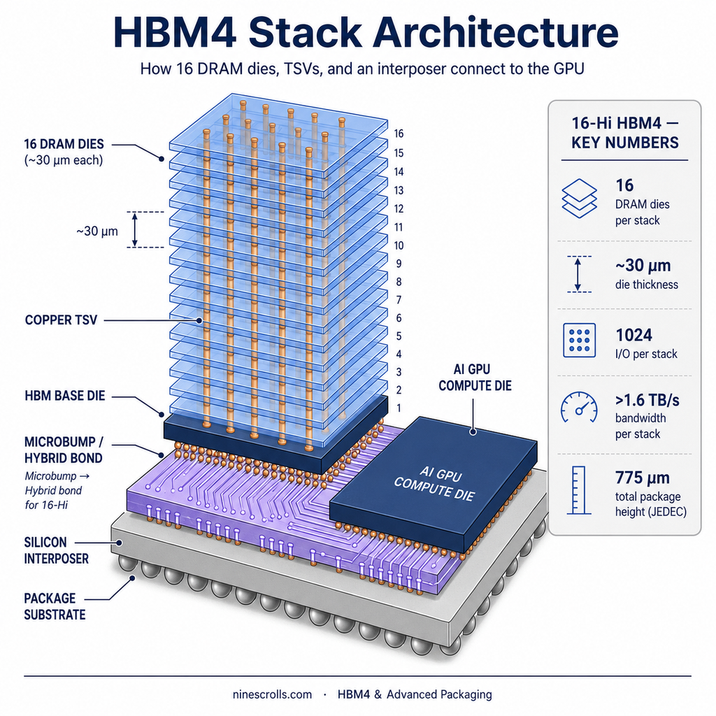
3. Why DRAM Dies Must Become Thinner
The fundamental problem is geometric. JEDEC caps HBM4 package thickness at 775 µm — only 50 µm thicker than HBM3E, and the standards body is widely expected to hold that ceiling for the 16-Hi variant. Adding four more die into the same height envelope forces every layer to shrink.
Current 12-Hi HBM uses DRAM die thinned to roughly 50 µm. Sixteen-Hi requires that to drop to approximately 30 µm — about a third the thickness of a human hair. Adhesive layers, currently around 10 µm, must shrink in lockstep. Hybrid bonding, where copper-to-copper interconnects replace solder microbumps entirely, becomes attractive precisely because it eliminates the bump and underfill stack-up.
Wafer thinning at this scale is not a backgrind problem in isolation. The handle wafer chemistry, the temporary bonding adhesive, the post-thinning stress and the through-silicon via reveal all become coupled. See Temporary Wafer Bonding and Debonding for the thin-wafer handling flow. TSV reveal — exposing the copper via tips on the thinned backside — requires controlled silicon recess by plasma etch, then PECVD passivation of the exposed copper, then chemical-mechanical polish — covered in full in TSV Reveal. The process window narrows dramatically as the die thins.
4. Thermal Bottlenecks in Stacked Memory
Sixteen DRAM die stacked at 30 µm each, plus thinned bonding interlayers, plus an HBM base die, fit inside roughly 775 µm of vertical budget. The thermal path from the upper die down through the stack to the substrate and out the package gets longer and more resistive with every added layer. Worse, the HBM stack sits on the same interposer as a multi-hundred-watt GPU, sharing a thermal interface that the cooling solution must service. The general reliability mechanisms behind this heat — temperature differential as stress — are covered in Reliability Challenges in High-Density 3D Packaging.
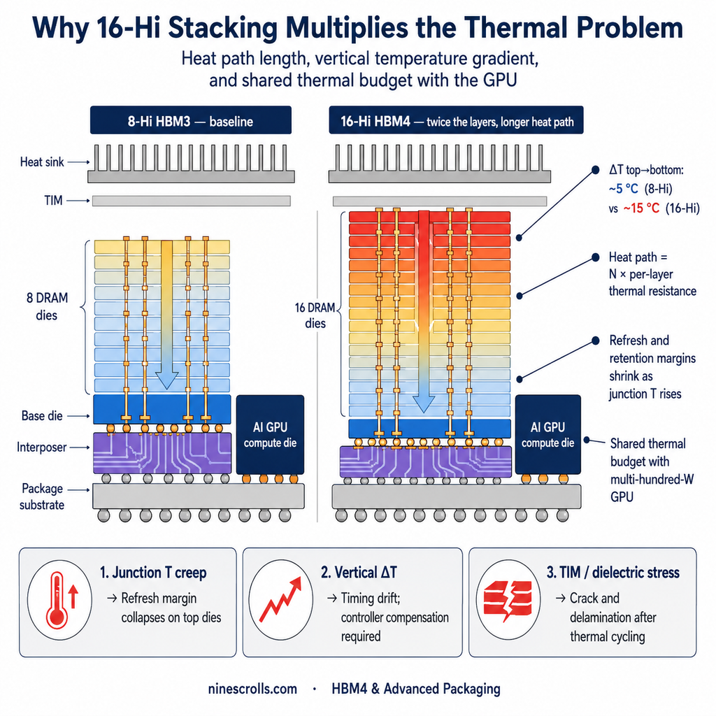
Three thermal failure modes dominate. First, junction temperature creep on the upper die degrades refresh and retention margins, which DRAM cannot tolerate. Second, thermal gradients between top and bottom layers create timing drift inside the stack that the memory controller must compensate for. Third, the interlayer thermal interface materials — adhesives, dielectrics, copper pads — accumulate stress under repeated thermal cycling and can crack or delaminate.
Solving this is not the memory team's problem alone. It pulls in materials science, dielectric thin-film engineering, plasma surface preparation and metrology. This is also exactly why UCLA's $125 million Semiconductor Hub, backed by Broadcom, Applied Materials, GlobalFoundries, Meta and Synopsys, names "thermal management" and "advanced packaging" alongside chip design as headline research thrusts.
5. Plasma-Activated Bonding
Hybrid bonding is the front-runner for 16-Hi and beyond. Samsung has indicated it will introduce hybrid bonding starting with its seventh-generation 16-layer HBM4E. SK hynix is developing hybrid bonding as a backup while pushing its MR-MUF approach as far as it will go. Either way, the industry is converging on a process where copper pads on the top wafer meet copper pads on the bottom wafer, surrounded by dielectric, with no microbump in between.
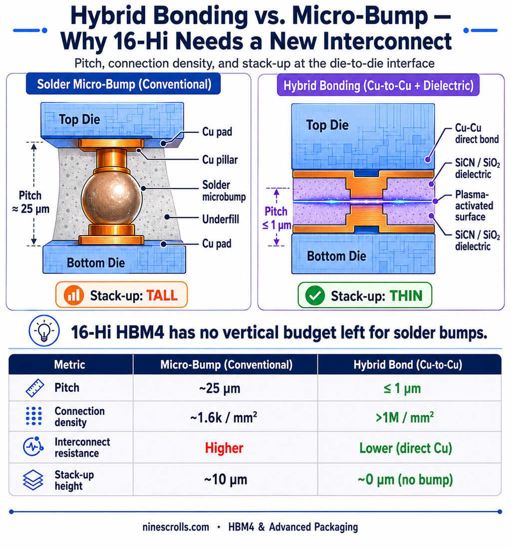
Plasma surface activation is the enabling step. Both wafer surfaces — typically silicon oxide or silicon carbon nitride dielectric with copper inlays — must be prepared so that dielectric-to-dielectric bonding forms at room temperature, and copper-to-copper diffusion bonding completes during the post-bond anneal. The activation step uses low-energy plasma (typically N₂, O₂ or H₂ chemistries) to terminate the dielectric surface with reactive species and to remove copper oxide from the pad tops. Surface roughness must hold below about 0.5 nm RMS for reliable void-free bonding.
This is a job for capacitively coupled or downstream plasma sources operated at low ion energy. Pattern damage and copper recess control are the dominant process specs. Equipment lines like NineScrolls' research-grade RIE and ICP-RIE platforms are increasingly being adapted for surface preparation rather than aggressive material removal — running short, soft plasma exposures with tightly controlled ion energies and well-characterized chemistry windows.
6. ALD Diffusion Barriers
At 30 µm wafer thickness with sub-micron TSV pitch in the hybrid-bonded interconnect, copper diffusion into surrounding silicon and dielectric becomes a reliability ceiling. Conventional PVD barrier-seed stacks struggle on the steep TSV sidewalls and on the narrow pad geometries that 16-Hi packing demands. Atomic Layer Deposition (ALD) is the natural answer.
Tantalum nitride (TaN), titanium nitride (TiN) and ruthenium ALD films, deposited at 200–350 °C with thicknesses of a few nanometers, give the conformal, pinhole-free coverage required to seal copper inside the via and the bond pad. ALD market data from multiple industry trackers project the segment growing from roughly $5.2 billion in 2025 to $12 billion-plus by 2035 — much of that growth tied directly to advanced packaging and memory.
For research and pilot lines exploring new barrier chemistries — for example ruthenium-tantalum bilayers, or self-aligned barriers grown by selective ALD — flexible, recipe-rich ALD systems with thermal and plasma-enhanced modes are the workhorse tool. Plasma-Enhanced ALD (PEALD) in particular allows lower deposition temperatures, which matters when the wafer underneath already carries thin DRAM die and temporary bonding adhesive.
7. Thin-Film Thermal Management
Once the stack is bonded, heat has to leave. Thin-film thermal management addresses three problem areas inside an HBM4 stack and the broader interposer.
First, dielectric selection. The interlayer dielectric (ILD) between bonded surfaces and around the copper interconnects acts as both an electrical insulator and a thermal resistor. Standard SiO₂ has poor thermal conductivity (~1.4 W/m·K). Silicon nitride is better. Silicon carbon nitride (SiCN), deposited by PECVD, is emerging as a preferred bonding dielectric for hybrid bonding precisely because it combines acceptable thermal conductivity with strong dielectric-to-dielectric bond strength after plasma activation. PECVD process control — temperature, RF power density, gas flow ratios — directly determines film density and therefore thermal conductivity.
Second, heat spreaders and integrated thermal layers. Diamond-like carbon (DLC), boron nitride (h-BN) and AlN films deposited by HDP-CVD or PECVD are being explored as on-chip or in-package heat spreaders. Conformal coverage over topography and low residual stress are the gating specs.
Third, surface coatings on package lids and TIM interfaces. Sputtered or ALD-grown adhesion layers between the die backside, the thermal interface material and the lid affect the interface thermal resistance that ends up dominating the package thermal budget. These films are thin, but the cumulative effect across a stack with 16 thermal interfaces is significant.
8. Advanced Packaging Implications
The HBM4 16-Hi transition is one input into a broader advanced packaging shift that the equipment industry is now structurally re-tooling around. TSMC has spelled out a CoWoS roadmap targeting over 14-reticle packages and 48× compute-density improvements by 2029, including support for 24-stack HBM5E. Applied Materials' acquisition of NEXX earlier this month positions it for panel-level electrochemical deposition, with substrate panels growing to 510 × 515 mm and beyond. Lam Research and Tokyo Electron are pouring R&D into hybrid bonding tools and high-aspect-ratio plasma etch for through-silicon and through-dielectric vias.
The common thread: every advanced packaging architecture currently being qualified depends on plasma processing for surface preparation, on PECVD or ALD for dielectric and barrier films, and on careful integration of those steps with mechanical thinning, bonding and reveal. The era when packaging was a back-end "after the fab" operation is over. Packaging is now a front-end-grade process flow, with front-end-grade equipment requirements. For the general selection framework between micro-bumps and hybrid bonding, see Hybrid Bonding vs Micro-Bump; for the vias that carry those signals through the silicon, see Through-Silicon Vias (TSV).
9. Equipment Requirements: Plasma Etch, PECVD, ALD
For research and development teams trying to qualify the materials and process steps that will eventually run in production HBM4 and HBM5 lines, the tool set looks like this:
Plasma etch. High-aspect-ratio TSV etch is the historical mainstay, served by deep reactive ion etch tools running Bosch or cryogenic chemistries. But hybrid bonding has driven a second use case: low-damage surface activation. ICP-RIE systems with tunable bias control and downstream plasma options support both — high-rate anisotropic etch for vias, soft surface treatment for bond prep. Research-grade RIE platforms remain critical for materials qualification work on new dielectric stacks and barrier candidates.
PECVD. The dielectric film stack — SiO₂, SiN, SiCN, low-k variants — is laid down predominantly by PECVD. For bonding dielectrics, film density, refractive index, residual stress and the surface chemistry after plasma activation are the parameters that decide whether a hybrid bond will void or survive thermal cycling. PECVD systems for R&D laboratories need multi-zone temperature control, dual-frequency RF and chemistry flexibility across silane, nitrous oxide, ammonia and organosilicon precursors.
HDP-CVD. For gap-fill in tight features and for stress-managed thick films used in some heat-spreader applications, high-density plasma CVD remains the workhorse. HDP-CVD systems sit in the toolset for institutes characterizing new fill chemistries or developing back-end-of-line stress engineering.
ALD. Atomic layer deposition covers the barrier, the seed precursor surfaces, and increasingly the bonding dielectric itself when sub-nanometer thickness control matters. Both thermal and plasma-enhanced ALD chambers are needed; flexible ALD systems with quick precursor swap and broad temperature range are the right fit for a lab investigating multiple material systems.
10. Outlook Toward HBM5 and Beyond
Even if 16-Hi HBM4 ships on the timeline NVIDIA is asking for, the trajectory does not slow. HBM5 is already on roadmaps targeting 16-Hi stacks with higher per-die capacity. HBM5E and HBM6 are anticipated to push to 20-Hi and 24-Hi over the coming decade. TSMC's CoWoS roadmap explicitly anticipates supporting 24 HBM5E stacks in a single package by 2029.
Every one of those generations will tighten the same three knobs: thinner wafers, denser interconnect, better thermal management. Each tightening pulls more weight onto plasma processing, thin film deposition and ALD. The UCLA Semiconductor Hub's research agenda — thermal management, advanced packaging, new materials, energy efficiency — is not coincidental positioning. It is an early signal that the next decade of memory and accelerator scaling will be a materials and process problem first, and a design problem second.
For research labs, university cleanrooms and corporate R&D groups setting up to work on these problems, the equipment selection question reduces to one criterion: can the tool hold a stable, well-characterized process window across the chemistry and temperature ranges that hybrid bonding, ALD barriers and PECVD bonding dielectrics demand? That is the lane NineScrolls' research-grade plasma etch, PECVD, HDP-CVD and ALD systems are built for.
Sources
- UCLA Samueli — $125 Million Semiconductor Hub launch announcement
- The Korea Herald — Nvidia's 16-layer HBM push raises stakes for memory chip-makers
- TweakTown — SK hynix, Samsung and Micron fighting for NVIDIA 16-Hi HBM4 orders
- CNBC — Meta, Broadcom and others to launch $125M semiconductor research hub at UCLA
- Tom's Hardware — TSMC next-gen CoWoS roadmap, 24 HBM5E stacks by 2029
- SEMI — Global 300mm fab equipment spending forecast
- Future Market Insights — Atomic Layer Deposition market forecast