Plasma Cleaner Applications: From Semiconductor Fabrication to Biomedical Devices
By NineScrolls Engineering · 2026-02-12 · 14 min read · Materials Science
Plasma cleaners are used across a wide spectrum of industries — anywhere surface cleanliness and activation are critical to product performance and reliability. This guide walks through the major application areas, explaining why plasma cleaning matters in each context and what specific processes benefit most from this technology.

Semiconductor and Microelectronics
The semiconductor industry is where plasma cleaning technology first gained widespread adoption, and it remains the largest application area today.
Wafer Surface Preparation
Before thin film deposition, lithography, or oxidation steps, silicon wafers must be free of organic contaminants, native oxides, and metallic impurities. Even sub-monolayer contamination can cause defects in nanometer-scale device structures. Oxygen plasma cleaning removes organic residues (such as photoresist remnants after ashing), while argon sputtering can strip thin native oxide layers before metal deposition.
In advanced nodes (7 nm and below), the tolerance for surface contamination is extremely tight. Plasma cleaning has become an essential in-situ step integrated directly into deposition and etch cluster tools, allowing wafers to be cleaned immediately before the next process step without breaking vacuum.
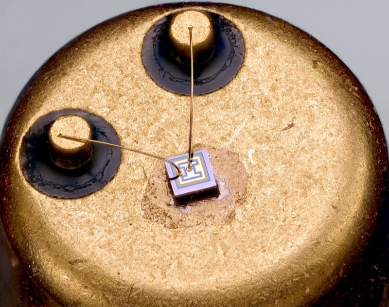
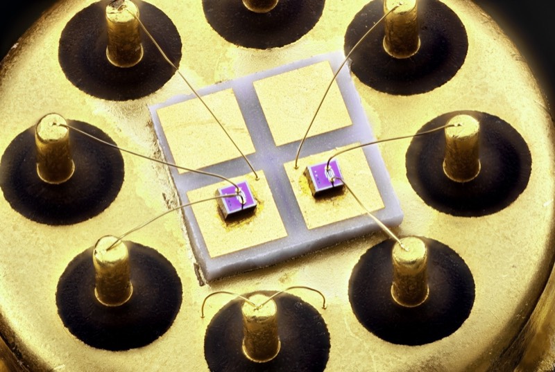
Wire Bonding and Die Attach
Wire bonding — the process of connecting IC chips to their package leads — is highly sensitive to surface contamination. Even trace amounts of organic residue on bond pads can cause bond failures, reducing yield and long-term reliability. A brief oxygen or argon plasma treatment (typically 1–3 minutes) before wire bonding dramatically improves bond pull strength and shear strength.
Similarly, die attach processes benefit from plasma-activated surfaces that improve adhesion of epoxy or solder materials to both the die and the substrate.
PCB and SMT Preparation
In printed circuit board (PCB) manufacturing, plasma cleaning is used to:
- Remove flux residues after soldering
- Activate copper surfaces before conformal coating or underfill
- Clean blind vias and micro-vias to ensure reliable plating
- Improve solder wettability on surface mount pads
For high-reliability applications (automotive, aerospace, medical), plasma cleaning of PCB assemblies is often a required process step rather than an optional one.
Medical Devices and Biomedical Engineering
The medical device industry relies on plasma cleaning for both contamination removal and surface modification — two capabilities that are especially valuable when working with implantable and diagnostic devices.
Implant Surface Treatment
Orthopedic implants, dental implants, and cardiovascular stents require surfaces that promote cell adhesion and osseointegration while remaining free of manufacturing residues. Plasma cleaning achieves both goals simultaneously: it removes machining oils and organic contaminants from titanium and stainless steel surfaces, and it increases surface energy to improve the wettability and biocompatibility of the implant.
Research has shown that oxygen plasma treatment of titanium implant surfaces can significantly enhance osteoblast adhesion and proliferation, leading to faster and more reliable integration with surrounding bone tissue.
Microfluidics and Lab-on-a-Chip
PDMS (polydimethylsiloxane) is the most common material for microfluidic devices, but its naturally hydrophobic surface creates challenges for fluid flow and channel bonding. Oxygen plasma treatment converts the PDMS surface from hydrophobic to hydrophilic by introducing polar functional groups (–OH), enabling:
- Irreversible bonding of PDMS to glass or PDMS-to-PDMS by activating both surfaces before contact
- Improved fluid flow characteristics in microchannels
- Better protein and cell adhesion for biological assays
This plasma bonding technique has become the standard method for fabricating microfluidic devices in research and commercial production.
Sterilization and Decontamination
Low-temperature plasma sterilization (using hydrogen peroxide or peracetic acid vapor activated by plasma) is used for heat-sensitive medical instruments that cannot withstand autoclave temperatures. Dedicated plasma cleaners using O₂ or Ar plasmas can serve as a pre-sterilization step to remove organic bioburden, improving the effectiveness of subsequent sterilization processes.
Optics and Display Manufacturing
Surface cleanliness is critical in optical applications where even nanometer-scale contamination can degrade performance.
Lens and Optical Component Cleaning
Before anti-reflection coating or other optical thin film deposition, glass and crystal substrates must be pristine. Plasma cleaning removes organic contaminants that would otherwise cause coating defects such as pinholes, delamination, or localized absorption. Common processes use O₂ or O₂/Ar plasma mixtures at moderate power to clean without roughening the polished optical surface.
Display Panel Preparation
In LCD and OLED manufacturing, plasma cleaning is used to prepare glass substrates and ITO (indium tin oxide) electrodes before alignment layer coating or organic layer deposition. The cleanliness and surface energy of ITO directly affect the uniformity of subsequent depositions and the electrical performance of the finished display.
Flexible display manufacturing on polymer substrates introduces additional challenges, as organic substrates are more sensitive to plasma damage. Low-power or remote plasma systems are preferred for these applications.
Automotive and Aerospace
These industries use plasma cleaning to meet stringent reliability requirements for adhesive bonding, coating adhesion, and long-term durability.
Adhesive Bonding Pre-Treatment
Modern automotive manufacturing increasingly relies on structural adhesive bonding to join dissimilar materials (aluminum to carbon fiber composites, for example). Plasma treatment before bonding improves adhesion strength by removing surface contaminants and creating chemical functional groups that form stronger bonds with the adhesive.
Compared to traditional surface preparation methods (solvent wiping, abrasive blasting), plasma cleaning is more consistent, automatable, and environmentally friendly — important factors in high-volume automotive production.
Aerospace Component Preparation
Aerospace applications demand exceptionally reliable bonds and coatings because failure in service can be catastrophic. Plasma cleaning is used before painting, primer application, and adhesive bonding of structural components. The aerospace industry also uses plasma treatment to prepare composite surfaces (such as CFRP) for secondary bonding, where the removal of release agents and the activation of the epoxy matrix surface are essential for bond integrity.
Materials Science and Research
Plasma cleaners are a standard piece of equipment in materials science laboratories, serving multiple purposes.
TEM and SEM Sample Preparation
Transmission electron microscopy (TEM) and scanning electron microscopy (SEM) samples are extremely sensitive to hydrocarbon contamination. Even trace amounts of organic material on a TEM grid can cause carbon buildup under the electron beam, degrading image quality and obscuring fine structural details. A brief (30–120 second) low-power plasma clean immediately before loading samples into the microscope removes these contaminants and dramatically improves imaging results.
Most TEM labs consider a plasma cleaner an indispensable companion to the microscope itself.
Surface Science and Thin Film Research
Researchers studying surface phenomena — catalysis, thin film growth, wetting behavior, surface chemistry — rely on plasma cleaning to produce well-defined, reproducible starting surfaces. By controlling gas chemistry and process parameters, researchers can not only clean surfaces but also introduce specific functional groups, allowing systematic study of surface chemistry effects.
Nanofabrication and MEMS
Micro-electromechanical systems (MEMS) fabrication involves many of the same processes as semiconductor manufacturing but often on substrates and structures that are more sensitive to contamination. Plasma cleaning is used throughout MEMS fabrication: before lithography to ensure photoresist adhesion, before etching to remove residues that could act as micro-masks, and before bonding to activate surfaces for wafer-level packaging.
Polymer and Textile Treatment
Plasma treatment is increasingly used for modifying polymer and textile surfaces without altering bulk material properties.
Polymer Surface Activation
Many engineering polymers (polyethylene, polypropylene, PTFE) have low surface energy, making them difficult to bond, print, or coat. Plasma treatment increases surface energy by introducing polar functional groups, enabling:
- Improved adhesion of adhesives and coatings
- Better ink wettability for printing
- Enhanced paintability without chemical primers
For PTFE — one of the most chemically inert polymers — plasma treatment is one of the few effective methods for improving adhesion without harsh chemical etchants.
Textile Functionalization
Atmospheric-pressure plasma systems are used in textile manufacturing to impart functional properties such as hydrophobicity, antimicrobial activity, or improved dye uptake. While this application typically uses atmospheric-pressure plasma jets rather than vacuum-based plasma cleaners, the underlying principles are the same.
Choosing the Right Process for Your Application
The optimal plasma cleaning process depends on several application-specific factors:
Contaminant type. Organic contaminants respond best to oxygen-containing plasmas. Inorganic contaminants or oxide layers may require argon sputtering or hydrogen reduction.
Substrate sensitivity. Delicate substrates (thin films, MEMS structures, polymer materials) require low-power or downstream plasma to minimize ion damage. Robust substrates (bulk metals, glass) can tolerate higher power and direct plasma exposure.
Required surface chemistry. If the goal is not only cleaning but also surface functionalization (e.g., making a surface hydrophilic), the choice of process gas directly determines the resulting surface chemistry.
Throughput requirements. High-volume production may benefit from inline or atmospheric-pressure plasma systems, while research and low-volume applications are well served by batch vacuum systems.
Beyond Cleaning: Plasma Surface Modification
Many of the applications above — PDMS bonding, paint adhesion, biomaterial preparation — are not strictly cleaning. They use the same low-pressure RF chamber to deliberately change the surface chemistry, raising surface energy, grafting specific functional groups (–NH₂, –CF₃, –COOH), or crosslinking the top nanometres. Where the goal is chemistry change rather than contaminant removal, the recipes, validation methods, and storage protocols are different. For a focused treatment of activation, functionalization, CASING crosslinking, hydrophobic-recovery countermeasures, and the cleaning-vs-modification boundary, see the dedicated Plasma Surface Modification practical guide.
Summary
Plasma cleaning technology serves a remarkably diverse range of industries, unified by a common need: atomically clean, chemically activated surfaces. Whether you are bonding semiconductor die, preparing medical implants, or activating polymers for coating, plasma cleaning offers a dry, residue-free, and highly controllable solution that is difficult to replicate with any other single technology.
The versatility of plasma cleaning — combined with its environmental advantages over wet chemical alternatives — continues to drive adoption in new application areas as manufacturing tolerances tighten and surface quality requirements increase across industries.
References
- Hegemann, D., Brunner, H. & Oehr, C. "Plasma treatment of polymers for surface and adhesion improvement." Nuclear Instruments and Methods in Physics Research B, 208, 281–286 (2003). doi:10.1016/S0168-583X(03)00644-X
- Chu, P. K., et al. "Plasma-surface modification of biomaterials." Materials Science and Engineering: R, 36(5–6), 143–206 (2002). doi:10.1016/S0927-796X(02)00004-9
- ASTM D2093-03: Standard Practice for Preparation of Surfaces of Plastics Prior to Adhesive Bonding. astm.org