Reactive Ion Etching (RIE) – Principles, Applications, and Equipment Guide
By NineScrolls Engineering · 2025-08-28 · 15 min read · Nanotechnology
Target Readers: Semiconductor/MEMS process engineers, equipment engineers, PIs/lab managers, R&D procurement teams, and technical decision-makers evaluating dry-etching solutions. Newcomers to plasma processing will find the fundamentals sections and glossary helpful; experienced engineers can skip to the process parameter tables and troubleshooting guide.
TL;DR Summary
- What it is: RIE combines chemical reactions with directional ion bombardment to pattern silicon, dielectrics, metals, and polymers with near‑vertical sidewalls.
- Levers that matter: pressure, RF power, gas chemistry, and substrate temperature — tuned together to balance etch rate, selectivity, and anisotropy.
- Three architectures: CCP‑RIE (cost‑effective, general‑purpose), ICP‑RIE (high density, independent ion energy, precision work), and DRIE/Bosch (deep Si, HAR > 20:1).
- What this guide delivers: plasma physics fundamentals, gas‑chemistry decision framework, starter process windows, troubleshooting reference, and equipment‑selection checklist.
1) What is Reactive Ion Etching?
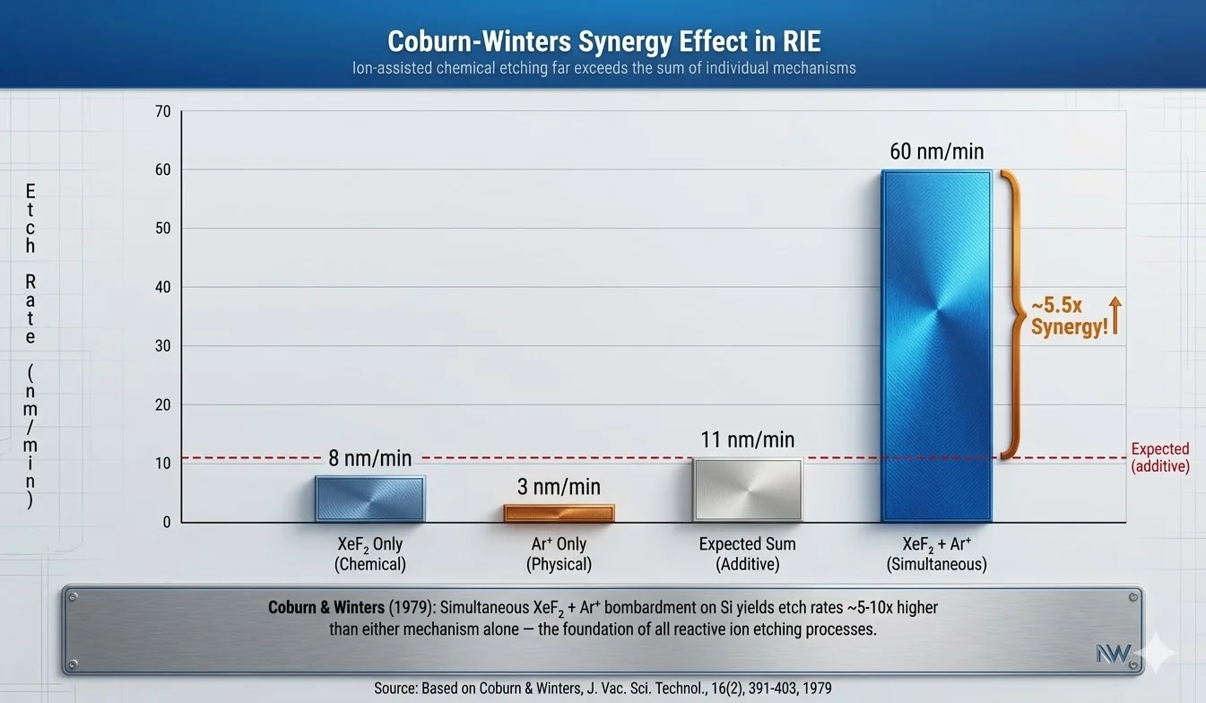
Reactive Ion Etching (RIE) is a dry‑etching technique in which a low‑pressure plasma of reactive gases is used to remove material from a substrate in a controlled, directional manner. Unlike isotropic wet etching (which undercuts mask features) or purely physical ion milling (which offers no chemical selectivity), RIE exploits the synergy between chemical volatilization and energetic ion bombardment — a phenomenon first quantified by Coburn and Winters in 1979. This synergy enables anisotropic profiles with high selectivity, making RIE indispensable for sub‑micron patterning.
RIE vs Other Etching Techniques
| Technique | Mechanism | Profile | Selectivity | Damage | Best For |
|---|---|---|---|---|---|
| Wet Etching | Chemical only | Isotropic | Very high | Minimal | Large features, cleaning, blanket strip |
| Ion Milling | Physical only (Ar⁺) | Anisotropic | Poor | High | Non-volatile materials (Pt, Au, ferrites) |
| Plasma Etching (PE) | Chemical (radicals) | Isotropic | High | Low | Resist strip, descum, surface cleaning |
| RIE | Chemical + physical | Anisotropic | Moderate–High | Moderate | Sub‑µm patterning, dielectric/Si etch |
| ICP‑RIE | Chemical + physical (high density) | Highly anisotropic | High | Low–Moderate | HAR structures, MEMS, advanced devices |
For a comprehensive comparison of these techniques — including reactor architectures, process parameters, and quantitative performance metrics — see our guide on Understanding the Differences: PE vs RIE vs ICP-RIE. For the chemistry-vs-physics decision in particular (when to use RIE versus pure ion bombardment for materials like noble metals or magnetic stacks), see RIE vs Ion Milling. And when the etched feature needs to be filled afterward, our HDP-CVD process guide covers void-free dielectric gap-fill for STI, TSV, and high-aspect-ratio trenches.
Brief History
RIE emerged in the late 1970s when researchers at Bell Labs and IBM recognized that placing the substrate on the powered electrode of a parallel‑plate reactor increased ion directionality dramatically. The landmark Coburn‑Winters experiment (1979) demonstrated that simultaneous Ar⁺ bombardment and XeF₂ exposure etched silicon up to 10× faster than either mechanism alone — establishing the theoretical foundation for all modern RIE processes.
2) Working Principle of RIE
2.1 Plasma Generation & Sheath Physics
In a typical parallel‑plate RIE reactor, an RF generator (usually 13.56 MHz) is connected to the bottom electrode (where the wafer sits) while the top electrode or chamber wall is grounded. When the RF field ionizes the process gas, a plasma forms consisting of:
- Ions: Positively charged species (e.g., CF₃⁺, SF₅⁺, Cl⁺) that provide directional bombardment
- Electrons: Highly mobile negative charges that sustain the plasma
- Radicals: Electrically neutral but chemically reactive fragments (e.g., F*, Cl*, O*) that drive chemical etching
- Photons: UV/visible emission from excited-state relaxation (basis for optical emission spectroscopy endpoint detection)
Because electrons are far more mobile than ions, they quickly charge the powered electrode negatively, creating a DC self‑bias (typically −100 to −500 V). This self‑bias accelerates positive ions across the plasma sheath toward the wafer surface, providing the directional energy that distinguishes RIE from isotropic plasma etching.

2.2 The Coburn‑Winters Synergy
The key insight behind RIE is that chemical etching and physical bombardment are not simply additive — they are synergistic. Ion bombardment enhances chemical etching by:
- Breaking surface bonds, creating dangling bonds for radical adsorption
- Removing inhibiting layers (e.g., native oxide, polymer passivation) from the trench bottom
- Locally heating the surface, accelerating desorption of volatile by‑products
- Providing directional energy — sidewalls receive minimal bombardment, so chemical passivation layers remain intact on vertical surfaces
This synergy is the reason RIE achieves anisotropic profiles with reasonable etch rates and good selectivity — something neither purely chemical nor purely physical methods can match.
2.3 By‑product Formation & Removal
For etching to proceed, the reaction products must be volatile so they can be pumped away. Common examples:
- Si + 4F* → SiF₄↑ (boiling point −86 °C, highly volatile)
- SiO₂ + CF₄ → SiF₄↑ + CO₂↑
- Al + 3Cl* → AlCl₃↑ (needs substrate heating >200 °C for adequate volatility)
- GaAs + Cl₂ → GaCl₃↑ + AsCl₃↑
If by‑products are non‑volatile (e.g., InCl₃ from InP etching in pure Cl₂), they re‑deposit as micro‑masks, causing surface roughening. In such cases, adding CH₄/H₂ chemistry or switching to BCl₃‑based processes is necessary.
3) Process Parameters & Control
RIE performance is governed by the interplay of five primary parameters. Understanding their interactions is critical for process optimization:
| Parameter | Effect on Etching | Typical Range | Trade‑off |
|---|---|---|---|
| Pressure | Controls mean free path (MFP) and ion directionality. Lower pressure → longer MFP → more anisotropic etch. | 5–200 mTorr | Low pressure improves anisotropy but reduces etch rate and may cause plasma instability. |
| RF Power | Sets plasma density and DC self‑bias. Higher power → more ions/radicals → higher etch rate and more physical sputtering. | 50–600 W (CCP‑RIE) | Higher RF increases etch rate but also increases damage, mask erosion, and heat load. |
| Gas Flow Rate | Determines radical supply, residence time, and by‑product removal efficiency. | 10–200 sccm | Too low → radical starvation and loading effects; too high → reduced residence time, wasted gas. |
| Gas Composition | Determines chemical selectivity, etch rate, and sidewall passivation behavior. | Application‑dependent | Adding O₂ increases F radical density but reduces polymer passivation; adding H₂/CHF₃ improves selectivity but reduces rate. |
| Substrate Temperature | Affects reaction kinetics, by‑product volatility, and sidewall passivation stability. | −20 to 80 °C (typical); up to 250 °C (metals) | Lower temp stabilizes sidewall polymer → better anisotropy; higher temp helps volatile by‑product desorption for metals. |

Parameter Interaction Guidelines
- Anisotropy optimization: Reduce pressure (5–30 mTorr) + moderate RF power + add passivation gas (CHF₃, C₄F₈) + cool substrate
- Selectivity optimization: Adjust gas ratio (e.g., increase CHF₃:CF₄ for SiO₂-over-Si selectivity) + reduce RF power to minimize physical sputtering
- Uniformity optimization: Tune gas distribution, pressure, and electrode gap; consider multi-zone gas injection
- Etch rate optimization: Increase RF power + pressure + reactive gas flow; ensure adequate by‑product pumping
4) Gas Chemistry Selection
Choosing the correct gas chemistry is the most critical decision in RIE process development. The guiding principle is simple: the etch product must be volatile at the process temperature. Below is a material-by-material guide:
4.1 Silicon Etching
| Gas System | Etch Product | Typical Rate | Profile | Notes |
|---|---|---|---|---|
| SF₆ | SiF₄ | 200–800 nm/min | Near-isotropic | Very high F radical yield; add O₂ for passivation or C₄F₈ for Bosch process |
| CF₄ / CF₄+O₂ | SiF₄ | 100–400 nm/min | Moderate anisotropy | O₂ addition scavenges CF₂ polymer, increasing free F; classic workhorse |
| Cl₂ / Cl₂+HBr | SiCl₄ | 100–500 nm/min | Highly anisotropic | HBr sidewall passivation gives excellent CD control; preferred for gate etch |
| SF₆/C₄F₈ (Bosch) | SiF₄ | 2–20 µm/min | Vertical (scalloped) | Alternating etch/passivation cycles; AR >20:1 possible; DRIE |
4.2 SiO₂ and Dielectric Etching
| Gas System | Selectivity (SiO₂:Si) | Notes |
|---|---|---|
| CHF₃ / CHF₃+CF₄ | 5:1 – 10:1 | H scavenges F, deposits polymer on Si but not on oxide → selectivity; workhorse for contact/via etch |
| C₄F₈ / C₄F₈+O₂+Ar | 10:1 – 20:1 | High selectivity for HAR oxide etch; used in ICP‑RIE for advanced via/trench |
| CF₄+H₂ | 8:1 – 15:1 | H₂ addition reduces F radical concentration → polymer deposition on Si surface → high selectivity |
4.3 SiNₓ Etching
- CF₄/O₂: Moderate selectivity over Si (~3:1); good rate; common for blanket SiNₓ removal
- CHF₃/O₂: Higher selectivity over SiO₂ (~5:1); useful for selective SiNₓ spacer etch
- CH₂F₂: High selectivity for SiNₓ over SiO₂ (up to 15:1); emerging for advanced spacer patterning
4.4 III‑V Compound Semiconductors & Metals
- GaAs/InP — Cl₂/BCl₃(/Ar): BCl₃ scavenges native oxide and provides Cl radicals; Ar enhances directionality. Substrate heating (60–200 °C) may be needed for InClₓ volatility.
- GaN — Cl₂/BCl₃(/N₂): Requires ICP‑RIE for adequate ion density; N₂ addition can improve surface stoichiometry.
- Al — Cl₂/BCl₃: Fast etch but Al forms non‑volatile Al₂O₃ native oxide; BCl₃ breaks through the oxide. Must handle corrosive AlCl₃ by‑products promptly (wafer rinse within minutes).
- W/Ti/TiN — SF₆/Cl₂: Fluorine‑based for W; chlorine‑based for Ti‑containing films.
Gas Selection Decision Guide
When developing a new RIE recipe, follow this decision framework:
- Identify the target material and confirm that volatile etch products exist at accessible temperatures
- Check selectivity requirements — what are the mask and stop-layer materials? Choose chemistry that deposits polymer or forms non‑volatile products on the layer you want to protect
- Determine profile requirements — if high anisotropy is needed, select chemistry with sidewall passivation capability (C₄F₈, HBr, CHF₃)
- Consider rate requirements — high F:C ratio gases (SF₆, CF₄) give fast rates; high C:F ratio gases (C₄F₈, CHF₃) give selectivity but lower rates
- Iterate with DOE — use 2–3 factor factorial design varying gas ratio, pressure, and RF power
4.5 Etch Rate & Selectivity Reference Matrix
The following table consolidates typical etch rates and selectivity ranges across the most common materials and chemistries. Values are starting-point ranges drawn from published literature and tool vendor data — actual results depend on chamber geometry, RF coupling, mask material, and feature loading.
| Material | Common Chemistry | CCP-RIE Rate | ICP-RIE Rate | Selectivity to PR | Selectivity to SiO₂ | Notes |
|---|---|---|---|---|---|---|
| Si | SF₆ / O₂ | 200–500 nm/min | 1–5 µm/min | 5:1 | high | Isotropic without bias; add C₄F₈ for sidewall passivation |
| Si (deep, Bosch) | SF₆ / C₄F₈ alternating | — | 5–20 µm/min | 80:1 | high | DRIE only; see DRIE Bosch process guide |
| Si (CMOS gate) | Cl₂ / HBr | 100–300 nm/min | 500–1500 nm/min | 30:1 | moderate | HBr enables vertical sidewalls and high selectivity to gate oxide |
| SiO₂ | CHF₃ / CF₄ / Ar | 50–150 nm/min | 200–600 nm/min | 3:1 | — | Self-passivating; ratio tunes selectivity |
| SiO₂ (HAR contact) | C₄F₈ / Ar / CO | — | 200–800 nm/min | 5:1 | — | For 10:1+ contact and via etch |
| Si₃N₄ | CHF₃ / O₂ or SF₆ | 50–200 nm/min | 200–500 nm/min | 3:1 | 2:1 | Selectivity to SiO₂ tunable via O₂ flow |
| GaN | Cl₂ / BCl₃ / Ar | — | 200–500 nm/min | 1:1 | low | HEMT mesa etch; metal mask preferred over PR |
| GaAs | Cl₂ / Ar or BCl₃ | — | 300–800 nm/min | 3:1 | low | Smooth profile; chamber temperature critical for AlGaAs stop layers |
| InP | Cl₂ / CH₄ / H₂ | — | 200–500 nm/min | 3:1 | low | Polymer formation risk; periodic O₂ chamber clean recommended |
| SiC | SF₆ / O₂ or NF₃ | — | 200–500 nm/min | 1:1 | moderate | Hard mask required (Ni, Al); slow because of high Si–C bond strength |
| Al / AlCu | Cl₂ / BCl₃ | 200–500 nm/min | 500–1000 nm/min | 5:1 | high | Post-etch passivation mandatory to prevent corrosion (H₂O + Cl residue) |
| Photoresist (strip) | O₂ | 200 nm – 1 µm/min | 1–5 µm/min | — | very high | For descum, drop power and time to 5–15 s at 30–50 W |
Reading the table: CCP rates are typical for parallel-plate RIE at 100–250 W; ICP rates assume an inductive source at 500–1500 W with independent bias. Selectivity to photoresist is for standard novolak/DUV resists; chemically amplified resists may degrade faster. For exact numbers on your tool, run a 2³ DOE varying pressure, power, and gas ratio against a witness wafer of known thickness.
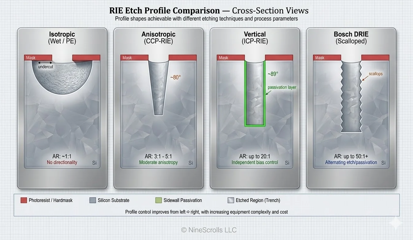
5) Types of RIE Systems
Three main RIE architectures exist, each with distinct plasma characteristics and application niches:
| Feature | CCP‑RIE | ICP‑RIE | DRIE (Bosch) |
|---|---|---|---|
| Plasma Source | Parallel‑plate RF (13.56 MHz) | Inductive coil (ICP source) + separate RF bias | ICP source with time‑multiplexed gas switching |
| Plasma Density | ~10⁹–10¹⁰ cm⁻³ | ~10¹¹–10¹² cm⁻³ | ~10¹¹–10¹² cm⁻³ |
| Ion Energy Control | Coupled to plasma density (single RF) | Independent (separate ICP + bias RF) | Independent per cycle phase |
| DC Self‑Bias | −100 to −500 V (high) | −10 to −200 V (independently tunable) | Varies per phase |
| Typical Etch Rate (Si) | 100–500 nm/min | 200–2,000 nm/min | 2–20 µm/min |
| HAR Capability | Up to ~5:1 | Up to ~20:1+ | Up to ~50:1+ (with optimization) |
| Substrate Damage | Moderate–High (ion energy coupled) | Low–Moderate (tunable) | Low–Moderate |
| Best For | General‑purpose etching, dielectrics, polymers, cost‑sensitive R&D | Precision patterning, III‑V etching, photonics, HAR structures, damage‑sensitive devices | MEMS, TSV, deep Si trenches, through‑wafer vias |
| Relative Cost | $ | $$ | $$$ |

Key distinction — independent ion energy control: In CCP‑RIE, a single RF source controls both plasma density and ion energy simultaneously, so increasing etch rate also increases ion damage. ICP‑RIE decouples these: the ICP coil sets plasma density (radical supply, etch rate) while a separate RF bias sets ion energy (directionality, damage). This independent control is why ICP‑RIE is preferred for damage‑sensitive or HAR applications.
HAR (High Aspect Ratio) explained: The aspect ratio is the depth‑to‑width ratio of an etched feature. A 1 µm wide trench etched 10 µm deep has an AR of 10:1. High‑AR etching is challenging because ions must reach the bottom of narrow features, and by‑products must escape. ICP‑RIE and DRIE are engineered to handle these challenges through high plasma density and passivation‑controlled sidewalls.
For a deeper dive into each system type, see our related guides: ICP‑RIE Technology Guide and DRIE – The Bosch Process Explained.
6) Applications of RIE
6.1 Semiconductor Device Fabrication
- Gate Patterning: Cl₂/HBr-based RIE for polysilicon gate etch with tight CD control (<1 nm variation). Endpoint detection via optical emission (SiCl* at 288 nm) ensures stopping precisely on gate oxide.
- Contact/Via Etching: CHF₃/CF₄/Ar for SiO₂ vias with high selectivity to Si. HAR capability (>10:1) requires ICP‑RIE with C₄F₈‑based chemistry.
- STI (Shallow Trench Isolation): Cl₂/O₂/HBr chemistry for Si trench etch (0.2–0.5 µm deep) with smooth sidewalls and minimal damage for subsequent oxide fill.
- Hardmask Opening: CF₄/CHF₃ for SiNₓ or SiON hardmask patterning prior to metal or dielectric etch.
6.2 MEMS & Microfluidics
- Deep Silicon Structures: DRIE (Bosch process) for pressure sensors, accelerometers, gyroscopes — features from 1 µm to >500 µm deep with near‑vertical sidewalls.
- Microfluidic Channels: Controlled etch depth and surface roughness using SF₆/C₄F₈ parameter tuning for channels in silicon or glass.
- Release Etch: XeF₂ or SF₆ plasma for isotropic undercut of sacrificial layers beneath MEMS structures.
6.3 Photonics & Waveguides
- Waveguide Fabrication: ICP‑RIE of SiO₂, SiNₓ, LiNbO₃, or III‑V materials to create low‑loss optical waveguides. Sidewall roughness <2 nm RMS is critical for minimizing scattering loss.
- Grating Structures: Shallow, highly uniform etch (<100 nm depth) for distributed Bragg reflectors and surface‑relief gratings.
- Photonic Crystals: Periodic hole arrays with sub‑wavelength dimensions require ICP‑RIE for precise profile control.
6.4 Power Devices & Compound Semiconductors
- SiC/GaN Etching: These wide-bandgap materials resist wet chemistry; RIE/ICP‑RIE with Cl₂/BCl₃/Ar is essential. SiC requires high ion energy due to strong Si‑C bonds.
- Mesa Isolation: Controlled depth etch to define active device regions in GaN HEMTs and SiC MOSFETs.
6.5 2D Materials & Emerging Applications
- Graphene Patterning: O₂ plasma for precise shaping of graphene channels. Very low power to avoid lattice damage.
- MoS₂/WSe₂ Device Fabrication: Gentle SF₆/Ar or XeF₂ etch to define transistor channels in TMD monolayers.
- Polymer & Organic Removal: O₂ or O₂/CF₄ plasma for resist stripping, surface functionalization, and cleaning.
6.6 TSV & Advanced Packaging
- Through‑Silicon Via (TSV): DRIE for vias 5–100 µm diameter, 50–300 µm deep in 3D IC integration.
- Redistribution Layer (RDL) Patterning: RIE of dielectric layers in fan‑out wafer-level packaging.
- Hybrid Bonding Surface Activation: Low-energy plasma prep of Cu pads and SiCN/SiO₂ dielectric before Cu-Cu hybrid bonding — see our HBM4 & Advanced Packaging guide for the 16-Hi HBM4 context.
7) Common Challenges & Troubleshooting
The following table covers the most frequently encountered RIE process issues, their root causes, and actionable solutions:
| Issue | Root Cause | Solution |
|---|---|---|
| RIE Lag (ARDE) | Narrower features etch slower because ions and radicals have difficulty reaching the bottom of narrow trenches; by‑products are slow to escape (aspect‑ratio‑dependent etching). | Lower pressure to improve ion directionality; increase bias; use ICP‑RIE for higher plasma density; optimize gas flow for efficient by‑product removal. |
| Micro‑masking | Non‑volatile etch by‑products or sputtered mask material re‑deposit as micro‑pillars ("grass") on the etch surface. | Reduce ion energy to minimize mask sputtering; add O₂ to volatilize organics; switch mask material (e.g., SiO₂ instead of metal); clean chamber more frequently. |
| Notching / Footing | Charge accumulation at insulator interfaces deflects ions sideways at the feature bottom, undercutting the profile. | Use pulsed bias or pulsed plasma to dissipate charge; reduce bias power; switch to ICP‑RIE with lower sheath voltage. |
| Sidewall Roughness | Mask edge roughness transfers into the etch; Bosch scalloping; inadequate passivation. | Improve mask (use hardmask, reduce LER); for Bosch, shorten cycle times; add passivation gas; consider cryogenic etch (−100 °C with SF₆/O₂). |
| Loading Effect | Etch rate varies with exposed area: more exposed material consumes more radicals, depleting them across the wafer. | Increase gas flow to ensure radical supply exceeds consumption; add dummy patterns to equalize open area; use endpoint detection per feature. |
| Selectivity Loss | Mask erodes faster than expected due to high ion energy or wrong chemistry; stop-layer is attacked. | Reduce bias power; increase polymer‑forming gas (CHF₃, C₄F₈); switch to harder mask (SiO₂, Cr, Ni); implement reliable endpoint detection. |
| Non‑uniformity | Uneven gas distribution, plasma asymmetry, or thermal gradients across the wafer. | Check showerhead clogging; verify electrode planarity and grounding; use multi-zone gas delivery; ensure good thermal contact (He backside cooling). |
| Plasma Damage | High‑energy ion bombardment causes lattice damage, trap states, or surface amorphization in the substrate. | Reduce DC self‑bias (use ICP‑RIE); use pulsed bias; lower RF power; implement soft‑landing endpoint strategy; consider post‑etch anneal. |
Prevention tips: Many of these issues can be avoided by establishing a robust SPC (Statistical Process Control) program — monitor etch rate, uniformity, and selectivity on dummy wafers before running device wafers, and track trends over time to catch chamber drift early.

8) Equipment Selection Checklist
Use the following checklist when evaluating RIE systems for your lab or fab:
8.1 Chamber & Reactor Design
- Chamber material: Anodized Al or ceramic‑lined for chemical resistance
- Electrode configuration: Parallel-plate (CCP) or ICP coil + separate bias electrode
- Wafer size compatibility: 2″ to 8″ (ensure platen/clamp compatibility)
- Chamber volume: Smaller chambers give faster gas residence time and better process control
8.2 RF System
- Source power: 300–3,000 W (ICP); 50–600 W (CCP‑RIE)
- Bias power: 0–600 W (separate for ICP‑RIE)
- Frequency: 13.56 MHz standard; some systems offer 2 MHz or 60 MHz for specific applications
- Matching network: Auto-match speed (<1 s typical); impedance range coverage
- Pulsed capability: Required for damage‑sensitive materials and charge‑neutralization (notching prevention)
8.3 Gas Delivery & Vacuum
- Number of gas lines: 4–8 MFC channels; ensure coverage for your target chemistries
- MFC accuracy: ±1% full scale at required flow ranges
- Vacuum system: Turbomolecular pump + dry backing pump for clean, oil‑free vacuum
- Base pressure: <5 × 10⁻⁶ Torr to minimize background contamination
- Pressure control: Throttle valve or conductance gate for stable process pressure
8.4 Wafer Handling & Temperature
- Loading: Open-load (simpler, lower cost) vs load‑lock (reduced moisture/O₂ exposure, better process stability)
- Substrate clamping: Mechanical clamp or electrostatic chuck (ESC); ESC preferred for uniform He backside cooling
- Temperature control: Chiller/heater range (−20 to 250 °C); He backside cooling for thermal uniformity
8.5 Process Monitoring & Endpoint Detection
- Optical emission spectroscopy (OES): Monitors plasma species in real time; essential for endpoint detection
- Laser interferometry: Measures etch depth in real time; useful for dielectric films
- Mass spectrometry (RGA): Residual gas analysis for by‑product monitoring and leak detection
- Data logging: All parameters (pressure, RF power, flow, temperature) logged for SPC and traceability
8.6 Safety & Compliance
- Gas safety: Toxic/flammable gas interlocks (Cl₂, BCl₃, SiH₄); gas cabinets with detection and auto‑shutoff
- Exhaust abatement: Wet scrubber or dry scrubber per gas chemistry requirements
- Facility requirements: Adequate exhaust, CDA, cooling water, electrical supply (208/480V)
- Regulatory compliance: SEMI S2/S8, NFPA, local codes
R&D vs Production Considerations
| Consideration | R&D / University | Production / Pilot Line |
|---|---|---|
| Flexibility | High priority — multi-material, frequent recipe changes | Less critical — dedicated to specific process |
| Throughput | Low (single-wafer OK) | High (load-lock, automation, fast pump-down) |
| Repeatability | Important but secondary | Critical — SPC, drift compensation |
| Budget | Cost-sensitive; open-load acceptable | Reliability and uptime justify higher cost |
9) Starter Process Windows
The following are non-production starting-point recipes for DOE development. Actual parameters depend on tool geometry, wafer size, and target specifications.
9.1 Silicon Etch (CCP‑RIE)
- Gas: SF₆ 30 sccm / O₂ 5 sccm
- Pressure: 30 mTorr
- RF Power: 100–200 W
- Temperature: 20 °C (chiller)
- Expected Rate: 200–400 nm/min
- Profile: Near-anisotropic with slight undercut
9.2 SiO₂ Etch (CCP‑RIE)
- Gas: CHF₃ 40 sccm / CF₄ 10 sccm / Ar 10 sccm
- Pressure: 40 mTorr
- RF Power: 150–250 W
- Temperature: 20 °C
- Expected Rate: 50–150 nm/min
- Selectivity (SiO₂:Si): ~5:1
9.3 Silicon Deep Etch (ICP‑RIE, Bosch)
- Etch step: SF₆ 100 sccm / 7 s / ICP 1,500 W / Bias 30 W / 20 mTorr
- Passivation step: C₄F₈ 80 sccm / 4 s / ICP 1,200 W / Bias 0 W / 15 mTorr
- Expected Rate: 5–10 µm/min
- Profile: Vertical with scalloping (scallop amplitude tunable via cycle time ratio)
9.4 Si₃N₄ Etch (CCP‑RIE)
- Gas: CHF₃ 30 sccm / O₂ 5 sccm
- Pressure: 30 mTorr
- RF Power: 100–200 W
- Temperature: 20 °C
- Expected Rate: 50–100 nm/min
- Selectivity (Si₃N₄:SiO₂): ~3:1 — increase O₂ flow to push selectivity higher at the cost of rate
9.5 GaN Mesa Etch (ICP‑RIE)
- Gas: Cl₂ 25 sccm / BCl₃ 5 sccm / Ar 10 sccm
- Pressure: 5 mTorr
- ICP Power: 500 W / Bias: 50 W
- Temperature: 60 °C (chuck warming reduces polymer)
- Expected Rate: 200–400 nm/min
- Profile: Vertical with smooth sidewall — critical for HEMT gate recess and laser facets. Use Ni or SiO₂ hard mask, not photoresist.
9.6 Photoresist Strip / Descum (CCP‑RIE)
- Gas: O₂ 50 sccm
- Pressure: 100 mTorr
- RF Power: 100–150 W (full strip) / 30–50 W (descum)
- Expected Rate: 500 nm/min – 2 µm/min depending on resist chemistry
- Note: For descum (removing residual scum after develop), run 5–15 s at low power. For full strip, time to clear plus 20% over-etch. Add 5% N₂ to reduce surface charging on dielectric stacks.
DOE Tip: Start with a 2³ factorial design varying pressure, RF power, and gas ratio. Measure etch rate (profilometer), selectivity (step height on two-layer test wafer), and profile (cross-section SEM). Iterate based on results.
10) Metrology & Validation
After etching, the following measurement techniques verify that the process meets specifications:
| Measurement | Technique | What It Tells You |
|---|---|---|
| Etch Depth / Rate | Stylus profilometer, optical profilometer | Step height and rate across wafer → uniformity |
| Sidewall Profile | Cross-section SEM (XSEM) | Sidewall angle, undercut, scalloping, roughness |
| CD / Feature Width | Top-down SEM, CD-SEM | Critical dimension accuracy and line-edge roughness (LER) |
| Film Thickness (remaining) | Spectroscopic ellipsometry | Remaining mask/stop-layer thickness → selectivity verification |
| Surface Composition | XPS, EDS | Residual polymer, contamination, surface chemistry changes |
| Surface Roughness | AFM | RMS roughness of etch floor (critical for photonics, MEMS) |
| Electrical Damage | CV, IV measurements | Interface trap density, leakage current — indicates plasma-induced damage |
Metrology selection tip: For routine process monitoring, profilometry + top-down SEM are sufficient. Add XSEM for profile development, ellipsometry for endpoint/selectivity verification, and AFM/XPS only when surface quality or contamination is a concern.
11) NineScrolls Etcher Portfolio
Our etching systems cover the full spectrum from general-purpose dielectric work to precision photonics and chemistry-free ion-beam milling. Backed by our manufacturing partner's three decades of semiconductor equipment experience and a global install base spanning leading research institutions, every configuration is tailored to specific material sets, throughput targets, and cleanroom constraints.
Equipment Comparison
| Specification | RIE Etcher | ICP Etcher | IBE / RIBE |
|---|---|---|---|
| Reactor Type | CCP parallel plate | ICP source + independent RF bias | Kaufman or RF ion source (beam) |
| Footprint (typical) | 1.0 m × 1.0 m | 1.0 m × 1.5 m | 1.0 m × 0.8 m |
| Wafer Size | 4 / 6 / 8 / 12″ or multi-wafer | 4 / 6 / 8 / 12″ or multi-wafer | Up to 6″ (Kaufman) · up to 12″ (RF) |
| RF Power | 300 – 1,000 W (single-source) | Source 1,000 – 3,000 W + Bias 300 – 1,000 W | Ion source dependent (swappable) |
| Gas Lines | 4 standard (customizable) | 5 standard + He backside (customizable) | 1 (Kaufman) or 3 (RF), customizable |
| Wafer Stage Temp | −70 °C to 200 °C | −70 °C to 200 °C | 5 – 20 °C (He backside optional) |
| Stage Motion | Fixed | Fixed | Tilt 0 – 90°, rotation 1 – 10 rpm |
| Vacuum | TMP + mechanical pump | TMP + mechanical pump | TMP + mechanical; base < 7×10⁻⁷ Torr |
| Non-Uniformity | < ±5% (edge exclusion) | < ±5% (edge exclusion) | < ±5% (edge exclusion) |
| Wafer Handling | Open-load or load-lock | Open-load or load-lock | Open-load or load-lock |
| Typical Materials | Si, SiO₂, SiNₓ, SiC, quartz, III‑V, metals, polymers | Si (DRIE/Bosch), SiO₂, III‑V, 2D materials, diamond, W/Ta/Mo | Metals, oxides, magnetic films, compound semiconductors (physical mill) |
| Best For | General-purpose R&D etching, dielectric patterning, resist stripping | Precision patterning, MEMS/DRIE, photonics, HAR structures, low-damage processes | Chemistry-free milling, sloped sidewalls, magnetic & optical device fabrication |
| Product Page | RIE Etcher → | ICP Etcher → | IBE / RIBE → |
Selecting the Right System
- Choose RIE Etcher if you need a cost-effective single-source CCP reactor for general dielectric and polymer work, teaching labs, or R&D groups running a broad mix of materials.
- Choose ICP Etcher if your workload demands independent control of plasma density and ion energy — DRIE/Bosch, III‑V and photonic materials, HAR features > 10:1, or charge-sensitive devices.
- Choose IBE / RIBE if you need chemistry-free physical milling, angled or sloped sidewalls, or material sets (permanent magnets, noble metals, multilayer stacks) that lack viable reactive chemistries.

Product pages: RIE Etcher · ICP Etcher · IBE / RIBE · 📥 Download full Equipment Guide (PDF)
12) Future Trends in RIE
12.1 Atomic Layer Etching (ALE)
ALE removes material one atomic layer at a time by alternating a self-limiting surface modification step (e.g., Cl₂ chemisorption) with a low-energy ion desorption step (Ar⁺ at 30–60 eV). Per-cycle removal is set by the saturated surface chemistry rather than by time, giving sub-Ångström control and near-zero CD bias. ALE is now in production for gate-all-around (GAA) transistor recess steps and advanced FinFET fin trim, and is being qualified for memory hole etch and EUV-mask defect repair. Throughput remains the main barrier — typical rates are 1–5 nm/min — so ALE is reserved for the most critical layers.
12.2 Pulsed Plasma & Pulsed Bias
Modulating either the source power or the bias power on millisecond time scales decouples ion flux from ion energy in a way that continuous-wave plasma cannot. Synchronous pulsing reduces charging damage on dielectric stacks, suppresses notching at SOI buried-oxide interfaces, and enables tighter control of sidewall passivation in HAR features. Pulsed-bias DRIE is now standard on advanced Bosch tools, and pulsed-source ICP is moving into mainstream III-V and photonic etch flows.
12.3 AI / ML-Assisted Process Optimization
Modern fabs and increasingly large R&D groups are training machine learning models on multi-variable process data — RF, OES spectra, MFC flows, chuck temperature, exhaust pressure — to predict optimal recipes, detect chamber drift before it produces bad wafers, and run virtual metrology that infers etch depth without physically measuring every wafer. Published case studies report development cycle reduction from weeks to days and yield recovery on aged chambers without preventive maintenance. Integration with run-to-run controllers and digital-twin chamber models is the next step.
12.4 Cryogenic Etching
Cooling the substrate to −100 to −120 °C with SF₆/O₂ chemistry produces a thin SiO_xF_y passivation layer that condenses on sidewalls but not the trench bottom (driven by ion bombardment), giving extremely smooth, scallop-free vertical sidewalls. Cryo is the production standard for damage-sensitive photonic Si waveguides and is gaining ground on Bosch for >50:1 aspect-ratio MEMS structures. The trade-off is added LN₂ infrastructure and tighter chuck temperature control.
12.5 Area-Selective Etching & Self-Aligned Patterning
Combining ALE with chemoselective surface functionalization (e.g., self-assembled monolayers that block one material but not another) produces inherent etch selectivity without lithographic masks. Early demonstrations on Si vs SiO₂ and metal vs dielectric stacks suggest a paradigm shift for self-aligned contact and via patterning at sub-3 nm nodes. Watch this space — material-selective ALE is one of the few credible paths to extending Moore's Law beyond what direct lithography can resolve.
13) FAQ
Q1: When should I choose ICP‑RIE over standard CCP‑RIE?
A: Choose ICP‑RIE when you need: (a) independent control of ion energy and plasma density, (b) high aspect ratio (>5:1) features, (c) low-damage etching for sensitive materials (III‑V, 2D materials, photonics), or (d) high etch rates with good uniformity. CCP‑RIE is sufficient for general-purpose dielectric/polymer etching, photoresist stripping, and applications where simplicity and cost matter more than ultimate performance.
Q2: How do I minimize plasma-induced damage?
A: (a) Use ICP‑RIE to decouple ion energy from plasma density — keep bias low while maintaining adequate radical supply. (b) Enable pulsed bias (duty cycle 10–50%) to reduce average ion energy. (c) Implement soft-landing: reduce bias power during the final 10–20% of etch time as you approach the stop layer. (d) Consider post-etch anneal (e.g., 400 °C in N₂/H₂) to recover lattice damage.
Q3: What endpoint detection method should I use?
A: OES (Optical Emission Spectroscopy) is the most versatile — monitor a characteristic emission line of an etch by‑product or reactant that changes when you reach the stop layer (e.g., SiF* at 777 nm drops when Si etch is complete). Laser interferometry is best for transparent film thickness monitoring (SiO₂, SiNₓ). For blanket etches without clear optical signals, use timed etch with a safety over-etch of 10–20%.
Q4: Can RIE etch high-aspect-ratio features?
A: Standard CCP‑RIE can achieve ~3:1 to 5:1 AR. For higher AR, ICP‑RIE extends this to ~20:1 through higher plasma density and independent bias control. For extreme AR (>20:1, up to 50:1+), DRIE (Bosch process) with alternating etch/passivation cycles is needed. The key limiting factors are ion angular distribution, radical transport into the feature, and by‑product removal.
Q5: How do I estimate equipment cost and CoO?
A: Equipment cost ranges from ~$100K–200K for a basic CCP‑RIE system to ~$300K–800K+ for a fully-loaded ICP‑RIE with DRIE capability. Cost of Ownership (CoO) includes: process gases (~$2K–10K/year depending on usage), pump maintenance (~$3K–5K/year), consumables (O-rings, clamp parts, liners: ~$2K–5K/year), and utilities (power, cooling water, CDA). For R&D labs running <20 hours/week, CoO is typically $15K–30K/year excluding the capital cost.
14) Glossary
- Anisotropy: Directional etching — vertical rate ≫ lateral rate, producing steep sidewalls
- ARDE (Aspect Ratio Dependent Etching): Phenomenon where etch rate decreases with increasing feature aspect ratio (also called "RIE lag")
- CCP: Capacitively Coupled Plasma — plasma generated between parallel-plate electrodes
- CD: Critical Dimension — the smallest feature width that must be controlled
- DC Self-Bias: Negative voltage that develops on the RF-powered electrode due to electron mobility asymmetry; accelerates ions toward the wafer
- DRIE: Deep Reactive Ion Etching — technique for etching deep (tens to hundreds of µm) high-AR features, typically using the Bosch process
- HAR: High Aspect Ratio — features where depth/width > 5:1
- ICP: Inductively Coupled Plasma — high-density plasma source using an RF-driven coil
- LER: Line Edge Roughness — random variation of feature edge position from ideal
- Loading Effect: Etch rate variation caused by differences in total exposed area across the wafer
- MFP: Mean Free Path — average distance a particle travels between collisions; determines ion directionality
- OES: Optical Emission Spectroscopy — technique for monitoring plasma composition via emitted light
- Selectivity: Ratio of etch rates between target material and mask/stop-layer (higher is better)
- SPC: Statistical Process Control — method for monitoring and controlling process stability over time
Call-to-Action
- Need help selecting between CCP‑RIE and ICP‑RIE for your specific materials and target CDs? Our process engineers can evaluate your requirements and recommend the optimal configuration.
- Want starter recipes and DOE templates for your materials? We provide process design kits for Si, SiO₂, III‑V, and photonic materials.
- Ready for a quotation? Contact us for configuration guidance, facility checklists, and budgetary pricing.
Contact:
RIE Etcher Series · ICP Etcher Series · Contact us · Email: info@ninescrolls.com
References
- Coburn, J. W. & Winters, H. F. "Plasma etching — A discussion of mechanisms." Journal of Vacuum Science & Technology, 16(2), 391–403 (1979). doi:10.1116/1.569958
- Jansen, H., et al. "A survey on the reactive ion etching of silicon in microtechnology." Journal of Micromechanics and Microengineering, 6(1), 14–28 (1996). doi:10.1088/0960-1317/6/1/002
- Donnelly, V. M. & Kornblit, A. "Plasma etching: Yesterday, today, and tomorrow." Journal of Vacuum Science & Technology A, 31(5), 050825 (2013). doi:10.1116/1.4819316
- Laermer, F. & Schilp, A. "Method of anisotropically etching silicon." U.S. Patent 5,501,893 (1996). (Bosch process patent)
- Winters, H. F. & Coburn, J. W. "Surface science aspects of etching reactions." Surface Science Reports, 14(4–6), 161–269 (1992). doi:10.1016/0167-5729(92)90009-Z
- Manos, D. M. & Flamm, D. L. Plasma Etching: An Introduction. Academic Press (1989). ISBN 978-0124693708.
- SEMI Standard E10-0304: Guide for Measurement of Plasma Etch Uniformity. semi.org