What Was Said, and Where
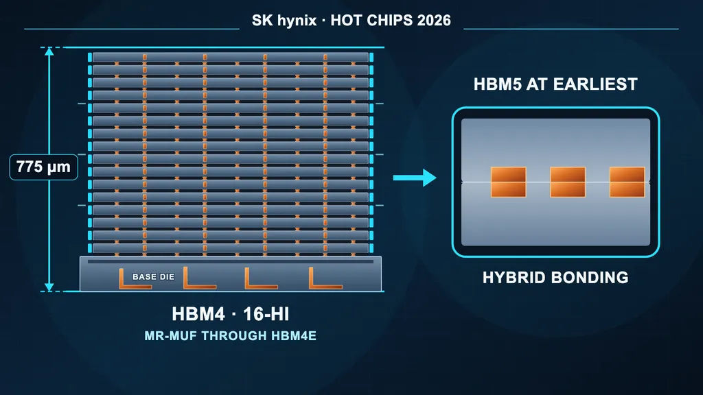
On August 23, 2026, Jaesik Lee, VP of package engineering at SK hynix America, presented the company's HBM packaging roadmap at Hot Chips 2026. The headline result for anyone building or specifying bonding equipment: SK hynix does not expect hybrid bonding to be ready for HBM4E, which pushes the transition to HBM5 at the earliest.
That is a notable statement from the vendor that holds roughly 70% of Nvidia's HBM orders for the Vera Rubin generation. All of that volume will ship stacked with mass reflow-molded underfill (MR-MUF), not copper-to-copper direct bonding.
It is also the counterpoint to Samsung's position. Samsung publicly committed to hybrid copper bonding for HBM4 in May 2025 and published system-level thermal modeling in June 2026 supporting the switch. SK hynix has held copper-to-copper as a backup behind advanced MR-MUF instead — and at Hot Chips it explained, in process terms, why the backup has not been promoted.
The 775-Micron Ceiling Is a Wafer-Thickness Constraint
The constraint driving the whole roadmap is a total package thickness of 775 microns. JEDEC raised the ceiling from 720 microns, which held through HBM3E, to 775 microns for HBM4.
The number is not arbitrary. When a GPU package gets its cold plate attached, both the logic die and the memory stacks are ground back to expose bare silicon. A standard 300 mm logic wafer is 775 microns thick, so a memory cube any taller would stand proud of the processor beside it. As Lee put it, that is the limit "because the logic wafer thickness is also 775 microns."
Every additional DRAM layer therefore has to come out of die thickness and gap height. HBM4 at 16-Hi — now in customer qualification at 48 GB per cube, with 12-Hi in mass production — thins its core dies to roughly 50 microns and halves the die-to-die gap relative to 12-Hi. SK hynix reports the same pattern on the earlier HBM3E 16-Hi transition: chip thickness, gap height, and bump pitch all cut approximately in half to fit two more dies into an unchanged Z-height budget.
Crucially, the JEDEC relaxation is what removed the immediate forcing function for hybrid bonding. Industry discussion now weighs a further move to 825–900 microns for 20-Hi stacks, which would push the copper-bonding crossover out again. Each time the ceiling has risen, micro-bump assembly has stayed viable for another generation.
Why MR-MUF Keeps Winning the Reprieve
SK hynix laid out the two incumbent die-to-die bonding options and their trade-off directly. Thermo-compression bonding with non-conductive film (TC+NCF) gives high productivity and low thermal resistivity but is sensitive to chip warpage. Mass reflow with molded underfill (MR+MUF) — which places all dies by pick-and-place, then joins them in a single reflow — handles thin-die warpage better, at the cost of higher thermal resistivity and a narrower gap-fill window.
That narrower window is exactly where 16-Hi hurts. Lee identified filling gaps that have shrunk by half while controlling warpage on sub-50-micron dies as the principal manufacturing challenge of the generation. This is the same class of problem covered in our discussion of 3D packaging reliability, where CTE mismatch and warpage across a thinned, multi-die stack become the limiting yield mechanism rather than any single interconnect step.
The thermal side compounds it. Thinner dies leave proportionally more oxide in the stack, and oxide conducts heat poorly compared with silicon. Pin speeds have risen from 1 Gbps in early HBM to 8 Gbps in HBM4, concentrating more power in the same footprint. SK hynix's own figures put the thermal burden 2.2× higher across the generations shown, while stack counts double every two generations. We have covered that thermal-and-materials wall in detail in the 16-Hi HBM thermal and materials analysis.
The Hybrid Bonding Numbers SK hynix Put on the Slide
SK hynix described the hybrid bonding mechanism the way the process actually runs: pick-and-place at room temperature to bring flattened copper pads and oxide surfaces into contact, then an anneal above 200 °C that forms SiO2-to-SiO2 and Cu-to-Cu bonds as the copper expands to close the recess. "This is a very simple process, but in reality it's really challenging," Lee said. "We are talking about 16 layers and 20 layers that we need to make the hybrid bonding, so it's very different from the one-layer stacking."
The payoff quantified on the deck, at 20-Hi: removing micro-bumps entirely lets core dies grow up to 24% thicker at the same Z-height, cuts thermal resistance by roughly 35% versus MR-MUF, and takes bump pitch below 18 microns against the roughly 30 microns where MR-MUF sits today. Hybrid bonding is positioned as the enabler for stacks of 20 layers and above.
The catch is the qualifier attached to that roadmap: for 20-plus-layer stacks, hybrid bonding remains at the research stage. At HBM4's current bump pitch, conventional micro-bumps still work — which is precisely the crossover logic laid out in hybrid bonding vs. micro-bump: the switch happens when pitch and thermal demands make bumps infeasible, not when the bonded interface is merely better. The physics of the bonded interface itself, including the contact step and the failure modes that dominate multi-layer stacking, is covered in our wafer bonding technologies guide.
Tooling is nonetheless moving. Industry sources reported in March 2026 that SK hynix placed its first mass-production hybrid bonding order — a single inline system pairing Applied Materials and Besi tools, worth roughly 20 billion won (about $15 million). Counterpoint Research expects the technique to enter full-scale HBM production with HBM5 around 2029–2030.
The Wafer-Level Flow Behind a Cube
The presentation was explicit that most of the HBM packaging challenge sits in wafer-level steps, not in the final assembly: TSV formation, micro-bumping, wafer thinning, and chip stacking. SK hynix flagged process uniformity, yield, and copper contamination as the concerns on the TSV and bump side, and thin-die handling plus warpage control on the thinning and stacking side.
HBM4 carries more than 20,000 TSVs and 16,148 base micro-bumps on a 12.8 × 11 mm part, targeting over 2 TB/s of bandwidth with a 40%-plus power-efficiency gain. Doubling TSV count is one of the two levers SK hynix named for the next generation — the other being more data I/Os and a faster per-I/O rate — alongside power TSVs distributed across the part for a claimed 75% power-delivery-network improvement. The via-formation and timing choices behind that count are the subject of our through-silicon via guide, and the plating step where uniformity and copper contamination are decided is covered in TSV copper fill.
The full flow runs silicon etch and TSV copper fill, BEOL metallization, wafer thinning, backside processing, singulation, and test — with a known-good stacked die (KGSD) wafer test inserted so that defective cubes do not consume expensive interposer area downstream. The backside thinning and reveal portion of that sequence is detailed in TSV reveal.
What This Does Not Settle
These are vendor slides and a conference Q&A, not a peer-reviewed result. The 24% thicker-die, 35% thermal-resistance, and 30%-plus i-HBM figures are SK hynix's own, measured against SK hynix baselines; the competing Samsung Heat Path Block and Micron base-die redesign claims are benchmarked on different metrics and are not directly comparable. Lee did not name a target generation for hybrid bonding — ruling out HBM4E leaves HBM5 as the earliest slot, but the company says the decision on which product moves first has not been made.
The i-HBM cooling concept, which embeds thermally conductive, electrically insulating blocks into the base die's die-to-die PHY region for a claimed 30%-plus thermal-resistance reduction, also carries a hard scheduling constraint: because the blocks sit inside the package alongside the D2D PHY, they require co-design with the customer and cannot be retrofitted to any generation already in design. Neither i-HBM nor Samsung's equivalent is expected in mass production before 2028.
One dissent is worth recording. During Q&A, Tanj Bennett of SemiAnalysis argued that stacking taller dilutes the silicon's own throughput: DRAM at the cell level delivers on the order of 20 TB/s per square centimeter, while a 20-Hi stack tops out near 4 TB/s, and HBM consumes far more manufacturing capacity than equivalent DDR5 or LPDDR. Lee's answer pointed toward tiering — keeping the KV cache in HBM and offloading to LPDDR — a split already visible in Nvidia's Vera Rubin platform and in the High Bandwidth Flash spec SK hynix co-developed with SanDisk.
NineScrolls Niche Angle
For plasma processing: The immediate read is that deep silicon etch demand is not slowing down — it is intensifying. More than 20,000 TSVs per HBM4 part, with TSV count identified as a primary lever for the next generation, means high-aspect-ratio via etch stays on the critical path regardless of which bonding method wins. Process uniformity across the wafer is the stated concern, and that is a profile-control problem in the etcher before it is an assembly problem. If hybrid bonding does arrive at HBM5, plasma work moves upstream rather than away: surface activation of the dielectric to produce a hydrophilic, -OH-terminated bonding surface becomes a yield-determining step, which we cover in surface preparation for Cu-Cu hybrid bonding.
For thin-film deposition: SK hynix's own thermal argument contains a deposition consequence that is easy to miss — thinner dies leave proportionally more oxide in the stack, and oxide is the poor thermal conductor in the path. Dielectric film thickness and quality in a thinned 16-Hi stack are therefore thermal parameters, not just isolation parameters. On the TSV side, the conformal liner and barrier films that precede copper fill get harder as aspect ratio rises and as copper contamination control tightens; that sequence is the front half of TSV copper fill.
For the equipment supply chain: The practical signal for anyone planning capital purchases is that the MR-MUF-to-hybrid-bonding transition is a moving target set partly by a standards committee, not purely by physics. Each JEDEC Z-height relaxation — 720 to 775 microns, with 825–900 microns under discussion for 20-Hi — buys micro-bump assembly another generation and defers bonder demand. Meanwhile the wafer-level tools feeding both paths, deep silicon etch, thinning and reveal, plating, and CMP, see demand either way. Labs and smaller fabs building 3D-integration capability should note that the front-end steps are the safe investment; the choice between bonding formats is separately argued in wafer-to-wafer vs. die-to-wafer.
Sources
- SK hynix HBM Packaging at Hot Chips 2026 — ServeTheHome, August 23, 2026
- Hot Chips 2026: SK hynix pushes hybrid bonding to HBM5 as AI memory hits 775-micron ceiling — Tom's Hardware, August 24, 2026
- Hot Chips 2026: Samsung's zHBM Claims 70% Power-Efficiency Gain; SK hynix Evaluates Intel EMIB — TrendForce, August 24, 2026
- Samsung pushes HBM toward logic, SK hynix targets packaging at Hot Chips — DIGITIMES, August 24, 2026