What Was Announced
On August 15, 2026, IEEE Spectrum published an interview with the two University of Michigan researchers leading "Common Earth," a project run in collaboration with imec to find substitutes for critical elements and fluorinated chemistries in semiconductor manufacturing. The leads are Valeria Bertacco, professor of computer engineering and vice provost, and John Heron, associate professor of materials science and engineering; imec's Jim Foresi is on the team.
What makes this worth a process engineer's attention is not the supply-chain framing — it is where the team says the exposure actually sits. Their two named targets are hafnium and, in Heron's words, "rare earth materials that are not directly integrated into the CMOS technology but facilitate the fabrication of the CMOS technology." That second category is process equipment hardware.
The Overlooked Dependency: Rare Earths Are in the Chamber, Not the Chip
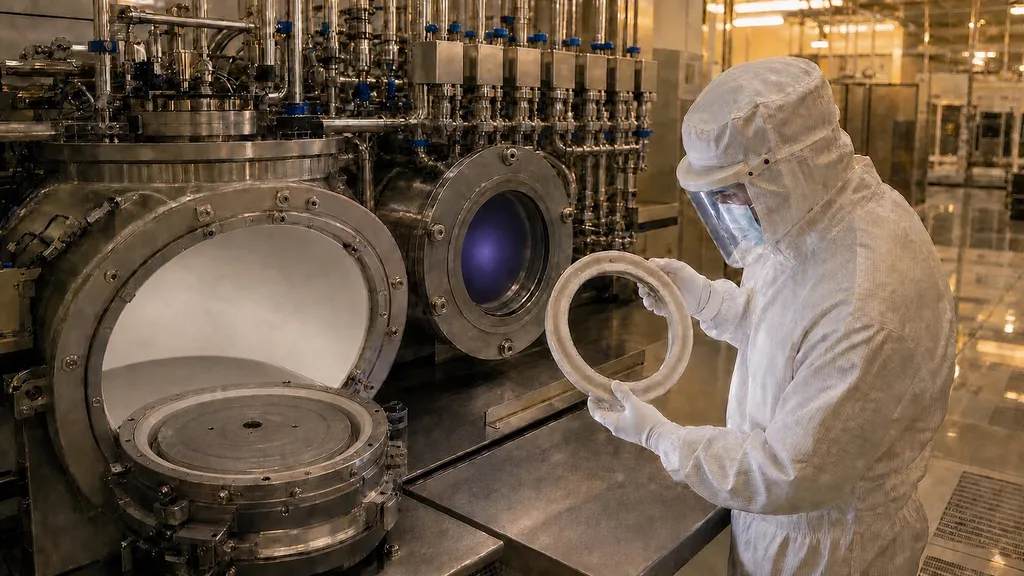
Heron is explicit about it: "The rare earth materials themselves show up typically in coatings for plasma-based deposition processes, so they're like barriers to protect equipment."
This is a well-established part of the plasma equipment supply chain that rarely makes the news. Yttrium oxide (Y2O3) is the reference material for halogen-plasma resistance, and yttria-coated surfaces have been reported to last roughly ten times longer in metal-etch plasma environments than high-purity alumina alone. The coatings go on chamber walls, dielectric windows, focus rings, capture rings and insert rings — and are increasingly applied by ALD rather than plasma spray for conformality on complex process-kit geometry. Lanthanide oxides (Ce2O3, Sm2O3, Gd2O3, Yb2O3) and rare-earth-doped zirconia-yttria formulations have all been described for the same duty.
Heron's point on sourcing is precise: "It's not that rare earths are rare on the planet, it's that the processing is most efficiently done with the ore that China has access to." The team's stated approach is to look for "other more accessible materials that are easy to refine, and trying to find those unique chemistries that are robust to these plasmas."
Hafnium: A High-k Precursor That Rides on the Nuclear Industry
The second target is hafnium, used in transistor gate dielectrics and deposited by ALD. Heron's supply-chain argument here is structural rather than geopolitical: hafnium is a byproduct of zirconium mining, and zirconium is mined for nuclear applications. "Some critical elements are byproducts of another industry," he says, "so if you want to scale semiconductor manufacturing, you basically have to scale a second industry."
The team is exploring "elemental alternatives to hafnium," with Heron pointing toward salt-based precursor routes. For anyone running high-k films, that lands squarely in precursor chemistry and ALD window definition — the material set covered in our atomic layer deposition guide.
Fluorine, PFAS, and the Etch Chemistry Problem
The third strand is fluorine. Perfluorocarbons and hydrofluorocarbons are the workhorses of directional dielectric etch and chamber clean; the fluorinated byproducts that leave the tool are classified as PFAS. Heron frames the regulatory risk bluntly: "If legislation comes down really hard and says, 'Hey, you can't have this waste product,' then that's basically going to be a knife to the heart if it doesn't get addressed."
Common Earth's stated process-level answer is a nitrogen-based precursor intended to eliminate fluorine from a deposition step, running in parallel with separate Michigan work on filtration to capture PFAS from the waste stream. Imec, per Heron, supplies both the manufacturing platform to test a new process and an existing division that classifies which PFAS uses are process-critical and which are not.
That classification work matters more than the substitution research in the near term, because fluorocarbon chemistry is not incidental to plasma etch — it is the mechanism. Fluorocarbon feed gases simultaneously etch and deposit a passivating polymer, and the balance between the two is what sets selectivity and sidewall profile. Anyone weighing a chemistry change should start from those fundamentals, which we cover in our reactive ion etching guide.
The Honest Trade-Off: Substitute Materials Are Worse Materials
Bertacco does not oversell the substitution. "There is a reason why people use a specific dielectric — because it provides the low latency and high performance that they need. Our solutions may be able to reach a good approximation, and they may actually have other potential positive traits, but they will be different."
Her proposed compensation is architectural: if a substitute dielectric leaks more, absorb it with better power gating, frequency throttling and circuit-level containment. The team is also pursuing chiplet-based "slice" designs to remove single-source dependencies at the design level. Bertacco cites the neon precedent — prices rose roughly tenfold when Ukrainian steel production, a major byproduct source, halted — as the model for how an unrelated industry can disrupt a fab overnight.
No performance data, coating-lifetime numbers, or process results were published with the interview. This is a research program with a stated direction, not a qualified alternative.
NineScrolls Niche Angle
For plasma processing: The story reframes rare-earth exposure as a consumables problem. Chamber liners, windows and focus rings are wear parts on a replacement cycle, so any change to the coating chemistry changes erosion rate, particle generation and mean time between wet cleans — all of which show up as process drift long before they show up as a hardware failure. Chamber erosion is driven by ion energy and ion flux, and those two knobs are set very differently across plasma regimes; if you are evaluating how a coating change would behave in your tool, start from the regime comparison in PE vs. RIE vs. ICP-RIE plasma etching. The plasma–surface chemistry that governs whether a candidate oxide survives halogen attack is the same chemistry described in our guide to plasma surface modification.
For thin-film deposition: Two deposition implications, pulling in opposite directions. Replacing hafnium touches the high-k ALD precursor set directly — a substitute must hold a real ALD window, self-limit cleanly, and deliver the k-value and leakage the device needs. See our ALD guide for what that qualification actually involves. At the same time, ALD is increasingly the method for applying rare-earth protective coatings to chamber hardware, so deposition is on both sides of this problem: the process being defended and the tool defending it.
For the equipment supply chain: A fluorine-free deposition precursor or a non-rare-earth chamber coating does not arrive as a drop-in. Each one is a requalification event — new gas delivery compatibility, new abatement duty, new particle and metals-contamination baselines, new process-kit lifetime data. Labs and fabs choosing tools today should be asking vendors what their coating and precursor roadmap looks like under a tightening PFAS regime, because the answer determines cost of ownership over the tool's life, not just at purchase. The underlying etch physics that any replacement chemistry has to reproduce is laid out in our RIE guide.
Sources
- Common Earth Project Aims to End Chip Supply Chain Bottlenecks — IEEE Spectrum, August 15, 2026
- imec's Michigan center — imec
- Removing PFAS from semiconductor manufacturing — imec
- Removing PFAS from Semiconductor Manufacturing: From Resists to Rinses — EE Times
- Semiconductor PFAS Consortium — Semiconductor Industry Association
- PFAS Explainer: Regulations for Semiconductor Manufacturing — SEMI
- Protecting Dry-Etch Chamber Parts Against Aggressive Plasma — Saint-Gobain Coating Solutions
- Yttria Oxide Ceramic — CoorsTek Technical Ceramics
- US8097105B2 — Extending lifetime of yttrium oxide as a plasma chamber material
- Electronic descriptors enable rational selection of plasma etching resistance in rare-earth oxide ceramics — ScienceDirect