What Was Published
On August 28, 2026, AIP published a Scilights summary (DOI 10.1063/10.0046481) of a new perspective paper in the Journal of Vacuum Science & Technology A: "Current status of atomic layer etching and its adoption to low-k fine patterning: An industrial perspective," by Sanghyun Lee, HyunWook Ra and Keun Hee Bai (DOI 10.1116/6.0005592). The paper is part of AIP Publishing's Atomic Layer Etching Collection.
The framing is deliberately not academic. Co-author Keun Hee Bai told AIP that "though academia has researched ALE, there are gaps in perspectives between [the research] and industry," and that the paper exists to close that gap — cataloguing the specific barriers that have kept ALE out of high-volume manufacturing and arguing they are being cleared.
The New Claim: Profile Verticality, Not Just Low Damage
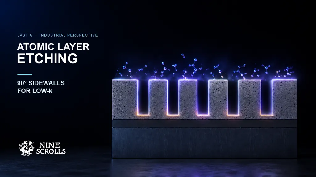
The standard case for ALE is three-part: low damage, high selectivity, fine thickness control. Lee et al. add a fourth. Per Bai, ALE "can create 90-degree angles with uniform widths into the layers" — the paper reports profile verticality as an independent advantage rather than a side effect of the other three.
That distinction matters commercially. Low damage and selectivity are electrical arguments that show up in device data. A vertical sidewall with uniform critical dimension through the depth of a feature is a patterning argument that shows up in overlay budgets and in whether a structure fits at all. Continuous reactive ion etching controls profile through a balance of ion bombardment and sidewall passivation that drifts with aspect ratio; a self-limiting cycle decouples removal from that balance.
Why ALE Has Not Displaced RIE Yet
The paper's stated limiting factors are low throughput and process complexity. AIP's summary reports the authors' central structural argument: the issues are not independent problems but a single collective challenge rooted in ALE's cyclical, multi-step nature. Every adsorption/removal cycle carries chamber purge and stabilization overhead, and the cost compounds linearly with the number of cycles.
The proposed remedies are process design and optimization plus architecture simplification — that is, reducing the number of distinct steps per cycle and the hardware required to execute them, rather than seeking a faster etch chemistry. This is a chamber-and-sequencing problem, not a chemistry problem.
The comparison baseline throughout is conventional reactive ion etching, which removes material fast and continuously through ion bombardment. Fabs are not choosing between ALE and nothing; they are choosing where in a stack to pay a cycle-time penalty for control. Readers weighing that trade should start with the regime distinctions in PE vs RIE vs ICP-RIE plasma etching, since the plasma density and ion-energy decoupling of an ICP-RIE platform is the hardware from which quasi-ALE and true ALE cycles are typically built.
Low-k Is the Wedge Application
The paper's title names the target explicitly: low-k fine patterning. Low-k dielectrics are the material where the conventional etch trade-off is worst — porous, carbon-doped films that lose carbon and take on moisture under energetic ion and VUV exposure, so the same bombardment that clears the feature degrades the dielectric constant the film was chosen for. Damage is not a yield abstraction here; it is the whole reason the material was specified.
That is what makes low-k the plausible first adoption beachhead rather than a general ALE rollout. Where damage cost is highest and etch depth is shortest, the cycle-count penalty is smallest and the payoff largest. The paper does not publish throughput figures or a node timeline, and the adoption claim is a perspective argument, not measured production data — that caveat should travel with the story.
NineScrolls Niche Angle
For plasma processing, the practical read is that ALE arrives as a mode of an existing tool, not a separate tool class. The cycle needs precise gas switching, fast chamber purge, low-energy well-controlled ion flux, and endpoint stability across hundreds of repetitions — all of which are ICP-RIE hardware attributes pushed to their tighter limits. Labs specifying a new etcher today should be asking about pulse and gas-switching latency, not only steady-state etch rate.
For process selection, the paper's verticality claim moves ALE into territory that has historically been handled by physical removal. When a project needs a truly anisotropic wall in a material that reacts badly to bombardment, the standing choice has been chemical versus physical — the trade-off laid out in reactive ion etching vs. ion milling. A self-limiting cycle that delivers a 90-degree profile without milling-level ion energy is a third option, and it is the one being argued for here.
For thin-film deposition, the coupling is direct: ALE and ALD share precursor delivery, purge, and self-limiting surface-reaction infrastructure, and low-k patterning depends on the deposited film stack as much as on the removal step. Fabs already carrying ALD capability carry most of the ALE learning curve with it.
For research groups, the throughput objection is close to irrelevant. A university or R&D lab running short depths at low wafer counts pays almost none of the cost that blocks high-volume adoption, which is why ALE process development has run ahead of production use — and why the gap Lee et al. describe between academic and industrial perspective exists in the first place.
Sources
- AIP Scilights — "Atomic layer etching brings 'cutting-edge' method to semiconductor nanofabrication," Ben Ikenson, August 28, 2026 (DOI 10.1063/10.0046481)
- Sanghyun Lee, HyunWook Ra, Keun Hee Bai, "Current status of atomic layer etching and its adoption to low-k fine patterning: An industrial perspective," Journal of Vacuum Science & Technology A (2026), DOI 10.1116/6.0005592
- AIP Publishing — Atomic Layer Etching (ALE) Collection