Wafer Loading Effect in Plasma Etching: Causes, Types, and Mitigation Strategies
By NineScrolls Engineering · 2026-04-03 · 14 min read · Materials Science
Target Readers: Semiconductor/MEMS process engineers, etch module engineers, integration engineers, and R&D scientists troubleshooting etch uniformity issues or developing pattern-density-sensitive processes. Engineers working on mixed-feature layouts (logic + memory, photonic + MEMS) or scaling to larger wafer sizes will find the quantitative models and mitigation strategies especially relevant.
TL;DR Summary
The wafer loading effect is a fundamental challenge in plasma etching: etch rate decreases as the total exposed area of etchable material increases, because reactive species are consumed faster than they can be replenished. This guide distinguishes three manifestations — macro loading (wafer-level), micro loading (pattern-level), and ARDE (aspect-ratio dependent etching) — explains the underlying physics of reactant depletion and byproduct inhibition, provides quantitative models for predicting loading magnitude, and offers actionable mitigation strategies spanning gas chemistry, chamber design, process tuning, and mask layout optimization. Whether you're diagnosing unexpected CD variation across a die or qualifying a new etch platform for mixed-density layouts, this guide provides the analytical framework and practical recipes to control loading effects.
1) What Is the Wafer Loading Effect?
In any plasma etching process, reactive species (radicals such as F*, Cl*, O*) are generated in the gas phase and transported to the wafer surface where they react with the exposed material. The wafer loading effect refers to the dependence of etch rate on the total area of material exposed to the plasma — when more material is exposed, more reactive species are consumed, reducing the local concentration of etchants and therefore the etch rate.
This effect was first systematically described by Mogab (1977), who observed that the etch rate of silicon in a CF₄ plasma decreased significantly as the number of wafers in a batch reactor increased. The phenomenon is not limited to batch systems: even in single-wafer reactors, pattern density variations across a die or wafer produce analogous effects at smaller scales.
Loading effects manifest at three distinct spatial scales, each with different physical origins and mitigation approaches:
| Type | Scale | Primary Mechanism | Observed As |
|---|---|---|---|
| Macro Loading | Wafer / chamber level | Global reactant depletion | Etch rate changes with exposed area, wafer count, or open area ratio |
| Micro Loading | Die / feature group level (µm–mm) | Local reactant depletion near dense features | Dense features etch slower than isolated features on the same die |
| ARDE | Individual feature level (nm–µm) | Knudsen transport limitation + ion angular distribution | Narrow/deep features etch slower than wide/shallow ones |
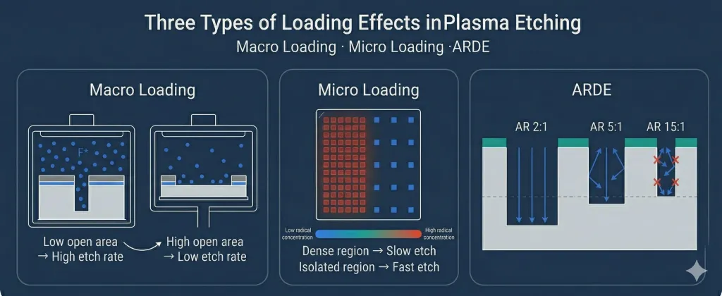
Figure 1: Three types of loading effects in plasma etching — macro loading (wafer-level), micro loading (die-level), and ARDE (feature-level) — each operating at different spatial scales with distinct physical mechanisms
2) Macro Loading: Wafer-Level Etch Rate Dependence
2.1 Physical Mechanism
Macro loading arises from a simple mass balance: reactive species are generated at a rate determined by the plasma source power and gas flow, but consumed at a rate proportional to the total exposed etchable area. When the consumption rate approaches the generation rate, the steady-state radical concentration — and therefore the etch rate — drops.
The classic Mogab model expresses this relationship as:
R = R₀ / (1 + k · As / V)
where R₀ is the unloaded etch rate (zero exposed area), As is the total exposed surface area, V is the chamber volume (proxy for radical generation), and k is a rate constant that encapsulates the sticking coefficient and reaction probability of the dominant radical species.
2.2 Practical Implications
- Open area ratio: A wafer with 80% photoresist coverage (20% open Si) etches faster than one with 20% coverage (80% open Si), even in the same chamber at identical process parameters
- Batch vs. single-wafer: In legacy batch systems, loading 25 wafers instead of 1 can reduce the etch rate by 30–50%. Single-wafer reactors largely eliminate this inter-wafer effect but remain susceptible to intra-wafer macro loading from pattern density variation
- Endpoint shift: Because etch rate varies with loading, time-based endpoint recipes are unreliable across different pattern densities. Optical emission spectroscopy (OES) or interferometric endpoint detection should be used instead
- Process qualification: Qualifying a recipe on blanket wafers and then applying it to patterned wafers often fails because the blanket condition represents maximum loading (100% open area)
2.3 Quantifying Macro Loading
The loading factor (LF) is defined as:
LF = (Rlow − Rhigh) / Rlow × 100%
where Rlow is the etch rate at low loading (small exposed area) and Rhigh is the etch rate at high loading (large exposed area). A loading factor below 5% is generally considered acceptable for production processes; research processes may tolerate up to 10–15% if uniformity is corrected by overetch.
3) Micro Loading: Pattern-Density Dependence
3.1 Physical Mechanism
Micro loading is the local analogue of macro loading: within a single die, regions with dense features (high local open area) consume reactive species faster than regions with isolated features (low local open area). Because radical transport from the bulk plasma to the wafer surface is primarily diffusion-limited, a concentration gradient develops — dense regions sit in a local "depletion zone" where radical concentrations are lower.
The characteristic diffusion length scale is:
λ = √(D / kr · ns)
where D is the radical diffusivity, kr is the surface reaction rate constant, and ns is the surface site density. For typical fluorine radical systems at 10–100 mTorr, λ ranges from 1–10 mm — meaning features separated by more than ~10 mm etch essentially independently, while features within this range influence each other.
3.2 Impact on CD Uniformity
Micro loading is one of the leading contributors to within-die CD (critical dimension) variation. Consider a logic die with both dense gate arrays (50% open area) and isolated I/O pads (5% open area):
- Dense gates etch slower → require more overetch time → increased sidewall tapering and potential punch-through of the underlying stop layer
- Isolated pads etch faster → reach endpoint first → experience longer overetch → lateral CD loss from continued isotropic etching
- The net result is a systematic CD offset between dense and isolated features that can reach 5–15 nm in advanced nodes — exceeding the CD uniformity budget
3.3 Micro Loading vs. Etch Bias
It is important to distinguish micro loading from etch bias (the difference between mask CD and etched CD at a given feature size). Etch bias arises from the balance of isotropic chemical etching and directional ion bombardment at the sidewall, while micro loading is a supply-limited phenomenon. However, the two effects compound: a feature in a dense region experiences both reduced etch rate (loading) and potentially different sidewall chemistry (because the radical-to-ion ratio changes with local radical depletion), making the profile more ion-dominated and more anisotropic — a sometimes-useful but difficult-to-control interaction.
4) Aspect Ratio Dependent Etching (ARDE)
4.1 Physical Mechanism
ARDE, also called RIE lag, describes the phenomenon where etch rate decreases as the aspect ratio (depth/width) of a feature increases. Unlike macro and micro loading, which are driven by lateral transport limitations in the boundary layer above the wafer, ARDE arises from transport limitations within the feature itself:
- Knudsen transport: At the low pressures used in RIE and ICP-RIE, the mean free path of gas molecules is comparable to or larger than the feature width. Radical transport into high-AR features becomes molecular (Knudsen) flow, where particles undergo random reflections from the sidewalls — each reflection has a probability of sticking and reacting, reducing the flux reaching the feature bottom
- Ion angular distribution: Ions entering a trench are collimated by the plasma sheath but still have a finite angular spread (typically ±2–5°). In high-AR features, only ions within a narrow acceptance cone reach the bottom; the rest hit the sidewalls, reducing the effective ion flux that drives anisotropic etching
- Byproduct redeposition: Volatile etch byproducts (e.g., SiF₄, SiCl₄) must diffuse out of the feature against the incoming flux of reactants. In high-AR features, byproducts can be re-deposited on sidewalls and the feature bottom, forming inhibiting layers that further reduce the etch rate
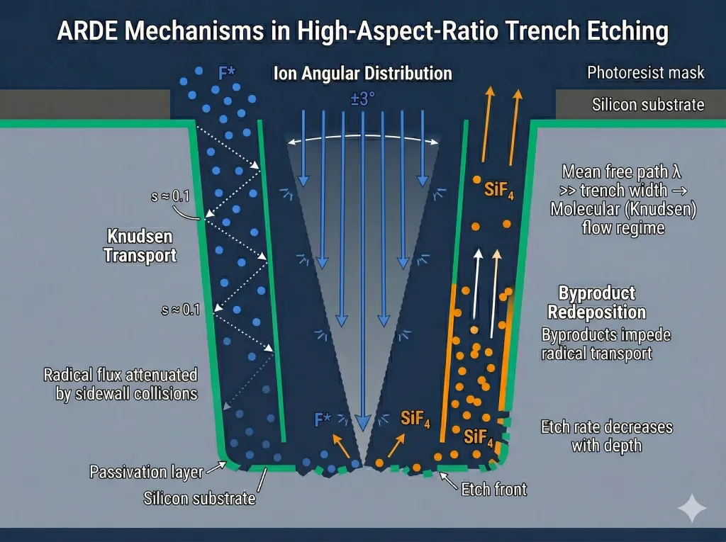
Figure 2: ARDE mechanisms inside a high-aspect-ratio trench — Knudsen transport limits radical delivery, ion angular spread reduces bombardment at the bottom, and byproduct redeposition creates inhibiting layers
4.2 ARDE in Practice
ARDE is particularly critical in DRIE / Bosch process applications where deep, narrow features are the objective. Typical examples include:
| Application | Typical AR | ARDE Severity | Impact |
|---|---|---|---|
| Through-silicon vias (TSVs) | 5:1 – 20:1 | Moderate–High | Depth variation across via sizes; bottom roughness |
| MEMS comb drives / accelerometers | 10:1 – 30:1 | High | Gap depth non-uniformity; device performance variation |
| Photonic crystal holes | 3:1 – 10:1 | Moderate | Hole depth variation affects optical performance |
| STI trenches (advanced CMOS) | 5:1 – 8:1 | Moderate | Trench depth variation across dense/ISO regions |
| HAR contact / via holes (DRAM, 3D NAND) | 40:1 – 100:1 | Extreme | Not-open contacts; bowing; twisting |
For a detailed treatment of the Bosch process and its interaction with ARDE, see our guide on Deep Reactive Ion Etching (DRIE).
4.3 Inverse ARDE
Under certain conditions — typically high ion energy, low pressure, and passivation-dominated regimes — the opposite trend can occur: wider features etch slower than narrower ones. This inverse ARDE (or inverse RIE lag) arises when sidewall passivation polymer is more effectively removed in narrow features (due to higher ion angular concentration) while wider features accumulate inhibiting layers on the bottom surface. Inverse ARDE has been exploited as a self-correcting mechanism in some cryogenic etch processes, where careful tuning of the passivation chemistry can produce near-zero net ARDE across a range of feature widths.
5) Material-Specific Loading Behavior
Loading effects are not universal across materials — the magnitude depends on the etch chemistry, the reaction probability (sticking coefficient) of the dominant radical, and the volatility of etch byproducts.
| Material | Common Chemistry | Dominant Radical | Loading Severity | Notes |
|---|---|---|---|---|
| Silicon | SF₆, CF₄, SF₆/C₄F₈ (Bosch) | F* | High | F* has high reaction probability with Si (~0.1); strong loading in pure SF₆ |
| SiO₂ | C₄F₈, CHF₃, CF₄/O₂ | CFx* | Moderate | Ion-assisted mechanism reduces pure chemical loading; polymer deposition adds complexity |
| Si₃N₄ | CHF₃/O₂, CH₂F₂ | CFx*, F* | Moderate–High | Selectivity to SiO₂ depends on loading-sensitive polymer balance |
| GaN / III-V | Cl₂/BCl₃, Cl₂/Ar | Cl* | Moderate | Cl* sticking coefficient on GaN lower than F* on Si; less severe loading but more surface damage sensitivity |
| SiC | SF₆/O₂, CF₄/O₂ | F* | High | Low etch rate makes loading effects proportionally significant; ion bombardment critical |
| Photoresist | O₂, O₂/CF₄ | O* | Very High | O* has very high reaction probability with organics; descum/strip processes highly loading-sensitive |
For a broader discussion of etch chemistry selection for emerging materials, see Etching Beyond Silicon. For selectivity considerations that interact with loading, see The Selectivity Challenge.
6) Mitigation Strategies
No single technique eliminates loading effects entirely — effective mitigation combines multiple approaches across gas chemistry, hardware, process tuning, and layout design.
6.1 Gas Chemistry Optimization
- Increase radical generation: Higher source power (ICP coil power) increases radical density, shifting the consumption-to-generation ratio and reducing loading. However, higher radical flux can degrade selectivity — balance is required
- Increase gas flow rate: Higher flow rates replenish consumed radicals faster, reducing the steady-state concentration drop. This also reduces residence time, which can affect polymer deposition in fluorocarbon chemistries
- Add diluent gases: Adding inert gases (Ar, He) increases total pressure without changing radical generation, improving gas-phase transport. He addition also improves wafer backside cooling uniformity
- Use less reactive chemistries: Replacing SF₆ (high F* yield, strong loading) with CF₄ or CHF₃ (lower F* yield, more polymerizing) reduces loading at the cost of etch rate. The trade-off is process time vs. uniformity
- Pulsed gas injection: In DRIE Bosch processes, optimizing the etch/passivation cycle timing can mitigate ARDE by adjusting the passivation removal rate at the feature bottom
6.2 Chamber and Hardware Design
- High-density plasma sources: ICP-RIE systems generate 10–100× higher radical densities than CCP-RIE, making the process less supply-limited and inherently less loading-sensitive. This is one of the primary reasons ICP-RIE has become the platform of choice for loading-critical applications
- Gas distribution design: Showerhead configurations with uniform gas injection across the wafer area reduce center-to-edge concentration gradients that compound with loading effects. Multi-zone showerheads allow tuning the radical supply profile
- Chamber volume: Larger chamber volumes provide a larger radical reservoir, reducing the fractional depletion caused by a given wafer load. However, larger volumes increase pump-down time and gas consumption
- Substrate temperature control: Uniform and stable wafer temperature (via electrostatic chuck with He backside cooling) ensures the surface reaction rate is constant across the wafer, preventing temperature-induced loading artifacts
6.3 Process Parameter Tuning
| Parameter | Effect on Loading | Trade-off |
|---|---|---|
| ↑ Source power (ICP) | Reduces macro/micro loading (more radicals) | May reduce selectivity; potential plasma damage |
| ↑ Bias power (RF) | Reduces ARDE (more directional ions penetrate high-AR features) | Increased mask erosion; higher surface damage; reduced selectivity |
| ↓ Pressure | Reduces ARDE (longer mean free path → more directional ions; less radical scattering) | Lower etch rate; may increase micro loading if radical generation drops |
| ↑ Gas flow | Reduces macro loading (faster radical replenishment) | Reduced residence time may affect polymer balance; higher gas cost |
| ↓ Temperature | Reduces chemical etch rate → shifts toward ion-driven regime → less loading | Lower throughput; may require cryogenic capability |
| Pulsed plasma | Allows radical replenishment during off-cycle; reduces ARDE and micro loading | Lower time-averaged etch rate; added process complexity |
6.4 Mask and Layout Design
- Dummy fill patterns: Adding non-functional features in low-density regions equalizes the local open area ratio across the die, dramatically reducing micro loading. This is standard practice in CMP (chemical-mechanical planarization) and increasingly adopted for etch uniformity
- Assist features: Sub-resolution assist features (SRAFs) used in lithography for OPC can also mitigate etch micro loading by locally increasing pattern density around isolated features
- Pattern density matching: Designing the mask so that critical features always appear in regions of similar local density minimizes loading-induced CD variation where it matters most
- Sacrificial open areas: For macro loading control, including sacrificial etch areas (e.g., in scribe lanes or die edges) can balance the total open area across different product wafers
6.5 Advanced Techniques
- Atomic layer etching (ALE): By separating the modification and removal steps, ALE achieves near-zero loading effects — each cycle removes exactly one monolayer regardless of pattern density. The trade-off is very low throughput (0.5–2 Å/cycle), making ALE practical only for thin films or critical layers
- Multi-step recipes: Using a high-power, low-selectivity "breakthrough" step followed by a low-loading main etch can improve uniformity for critical layers
- Real-time feedback control: Advanced etch platforms use in-situ OES, ellipsometry, or interferometry to detect loading-induced rate changes and adjust power/flow in real time. This closed-loop approach is especially valuable for DRIE processes where ARDE accumulates over hundreds of cycles
- Machine learning optimization: ML-based process optimization can model the complex interactions between loading, process parameters, and feature geometry to find operating points that minimize loading across all feature types simultaneously
7) Diagnosing Loading Effects in Your Process
When etch uniformity issues arise, systematically identifying whether loading is the root cause — and which type — is critical for choosing the right mitigation strategy.
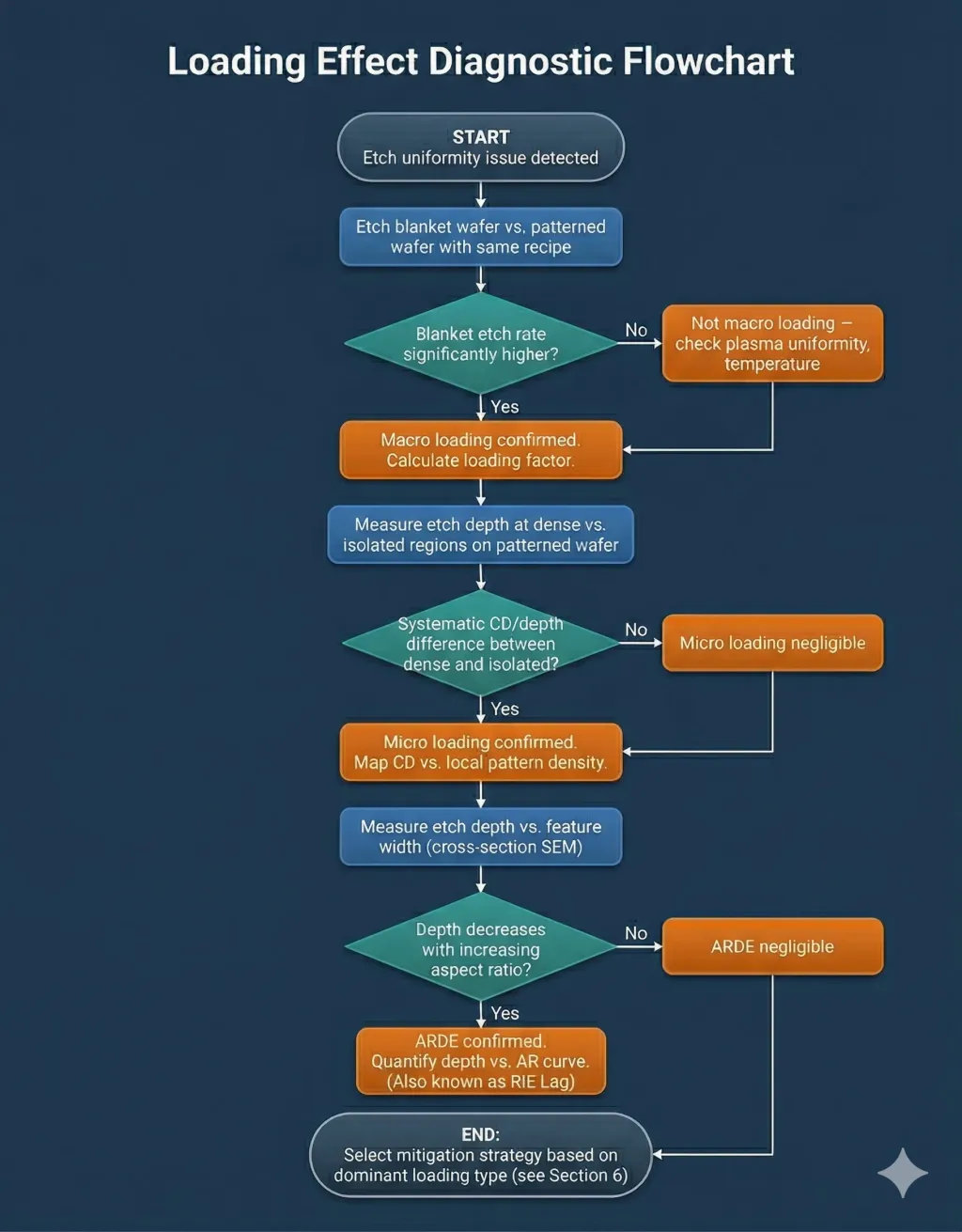
Figure 3: Loading effect diagnostic flowchart — systematic procedure to identify whether macro loading, micro loading, or ARDE is the dominant contributor to etch uniformity issues
7.1 Diagnostic Procedure
- Blanket vs. patterned comparison: Etch a blanket (unpatterned) wafer and a patterned wafer with identical process parameters. If the blanket wafer etches significantly faster, macro loading is present. Quantify the loading factor as described in Section 2.3
- Dense vs. isolated measurement: On the patterned wafer, measure etch depth (or remaining film thickness) at dense-feature regions and isolated-feature regions. A systematic difference indicates micro loading. Map the CD or depth across the die to visualize the loading pattern
- Feature-width dependence: Measure etch depth as a function of trench width (for a constant pitch) or feature aspect ratio. If depth decreases monotonically with increasing AR, ARDE is present. Cross-section SEM is the most reliable measurement for this
- Endpoint analysis: If your system has OES endpoint detection, monitor the endpoint signal intensity — a gradual, rounded endpoint rather than a sharp drop suggests significant loading-induced etch rate variation across the wafer
- Wafer-level uniformity mapping: Use a 49-point or higher-resolution ellipsometry or profilometry map to separate center-to-edge non-uniformity (plasma non-uniformity) from pattern-correlated non-uniformity (loading). If the map correlates with the pattern density distribution, loading is the dominant factor
For a broader treatment of plasma non-uniformity causes and diagnostics, see Why Plasma is Non-Uniform in Etch Chambers.
7.2 Common Misdiagnoses
- Loading vs. plasma non-uniformity: Both cause etch rate variation across the wafer, but plasma non-uniformity produces a radial pattern (center-to-edge) while loading produces a pattern that correlates with local feature density. Running the same process on a blanket wafer distinguishes the two
- Loading vs. temperature non-uniformity: Poor wafer clamping or non-uniform He backside pressure can create localized hot spots with higher etch rates, mimicking inverse loading. Verifying chuck performance with a thermal test wafer rules this out
- ARDE vs. incomplete etch: When narrow trenches appear shallower than wide ones, confirm that the wide trenches have not etched through the target film and stopped on an underlying layer. What appears to be ARDE may actually be endpoint-limited etching in the wide features
8) Loading Effects Across Reactor Architectures
The severity and character of loading effects varies significantly across different plasma reactor types:
| Reactor Type | Macro Loading | Micro Loading | ARDE | Why |
|---|---|---|---|---|
| CCP-RIE | High | High | Moderate | Low plasma density → limited radical supply → strong depletion effects |
| ICP-RIE | Low–Moderate | Low–Moderate | Moderate | High plasma density → abundant radical supply; independent bias control helps ARDE |
| DRIE (Bosch) | Low | Moderate | High | ICP source minimizes macro loading; cyclic process accumulates ARDE over hundreds of cycles |
| Cryogenic ICP | Low | Low | Low–Moderate | Continuous etch avoids Bosch ARDE accumulation; passivation tuning can achieve inverse ARDE compensation |
| ALE | Minimal | Minimal | Minimal | Self-limiting monolayer removal inherently eliminates loading dependence |
9) Frequently Asked Questions
What is the difference between wafer loading and plasma non-uniformity?
Plasma non-uniformity is a property of the reactor — it exists even with a blanket (unpatterned) wafer and typically produces a radial (center-to-edge) etch rate profile. Wafer loading is pattern-dependent — it produces etch rate variation that correlates with the local or global density of exposed material. To distinguish them, etch both a blanket wafer and a patterned wafer: the blanket wafer shows only plasma non-uniformity, while the patterned wafer shows the combination of both effects. The difference between the two maps isolates the loading component.
Can loading effects be completely eliminated?
In conventional continuous plasma etching, loading effects cannot be fully eliminated — only minimized. High-density plasma sources (ICP), high gas flows, and dummy fill patterns can reduce the loading factor to below 5%, which is acceptable for most applications. The only technique that fundamentally eliminates loading is atomic layer etching (ALE), where the self-limiting reaction mechanism removes a fixed amount of material per cycle regardless of the exposed area. However, ALE's low throughput limits its use to thin-film applications or the most critical process layers.
How does loading affect endpoint detection?
Loading causes different regions of the wafer to clear at different times, producing a "smeared" endpoint signal. In OES-based detection, the emission intensity change at endpoint becomes gradual rather than sharp, making it harder to determine the exact moment to stop. This is why loaded processes require a controlled overetch step — typically 10–30% of the main etch time — to ensure all regions clear. Using interferometric endpoint on a specific test structure in a representative density region provides more reliable endpoint than global OES for heavily loaded processes.
Why does my blanket etch rate not match my patterned wafer etch rate?
This is the classic macro loading effect. A blanket wafer exposes 100% of the surface to the plasma, consuming the maximum amount of reactive species. A patterned wafer with, say, 30% open area consumes only 30% as many radicals, resulting in a higher local radical concentration and faster etch rate in the open regions. The difference can be 20–50% depending on the chemistry and reactor type. Always qualify your process on patterned test wafers that match your production pattern density, or use a loading correction factor derived from blanket-to-patterned comparison.
Is loading worse at lower pressure?
It depends on the type of loading. Lower pressure typically reduces ARDE because the longer mean free path produces more directional ions that can reach the bottom of high-AR features. However, lower pressure can increase macro and micro loading if the total radical generation rate drops (fewer collisions to sustain ionization). ICP sources are less sensitive to this trade-off because the inductive coupling maintains high plasma density even at low pressure — another advantage of ICP-RIE for loading-sensitive processes.
How do I minimize loading effects when etching silicon in SF₆?
SF₆-based silicon etching is particularly loading-sensitive because fluorine radicals have a high sticking coefficient on silicon (~0.1). Key mitigation strategies: (1) Use an ICP source to maximize radical generation — the high plasma density provides a larger radical "budget" that is less affected by consumption. (2) Increase SF₆ flow rate to improve radical replenishment. (3) Add O₂ (5–20%) to form a thin SiOxFy passivation layer that slows the chemical etch rate and shifts the process toward a more ion-driven, less loading-sensitive regime. (4) Lower the process pressure (5–15 mTorr) to improve ion directionality and reduce ARDE. (5) Consider a mixed-mode etch (SF₆/C₄F₈ without cycling) if your application allows it — the continuous passivation component reduces the loading sensitivity compared to pure SF₆.
10) Key Takeaways
- Loading is inherent to plasma etching — whenever reactive species are consumed by the substrate, the etch rate depends on how much substrate is exposed. The goal is to minimize and control loading, not to assume it can be ignored
- Three scales, three mechanisms: macro loading (global depletion), micro loading (local depletion), and ARDE (in-feature transport) require different mitigation strategies
- ICP-RIE is inherently less loading-sensitive than CCP-RIE due to 10–100× higher radical density — this alone can reduce macro and micro loading to acceptable levels for many applications
- ALE is the only loading-free approach but is limited by throughput. For most processes, the practical solution is a combination of high-density plasma, optimized gas chemistry, appropriate pressure, and layout-level dummy fill
- Always qualify on representative patterns — blanket wafer results do not predict patterned wafer behavior when loading is significant
- Diagnose before you mitigate — use the systematic diagnostic procedure (Section 7) to identify which type of loading is dominant before adjusting process parameters
References
- C. J. Mogab, "The Loading Effect in Plasma Etching," J. Electrochem. Soc., vol. 124, no. 8, pp. 1262–1268, 1977
- J. W. Coburn and H. F. Winters, "Ion‐ and electron‐assisted gas‐surface chemistry — An important effect in plasma etching," J. Appl. Phys., vol. 50, no. 5, pp. 3189–3196, 1979
- R. A. Gottscho, C. W. Jurgensen, and D. J. Vitkavage, "Microscopic uniformity in plasma etching," J. Vac. Sci. Technol. B, vol. 10, no. 5, pp. 2133–2147, 1992
- K. P. Giapis and G. S. Hwang, "Pattern-dependent charging and the role of electron tunneling," Jpn. J. Appl. Phys., vol. 37, pp. 2281–2290, 1998
- M. A. Blauw, T. Zijlstra, and E. van der Drift, "Balancing the etching and passivation in time-multiplexed deep dry etching of silicon," J. Vac. Sci. Technol. B, vol. 19, no. 6, pp. 2930–2934, 2001
- H. Jansen et al., "Black silicon method X: a review on high speed and selective plasma etching of silicon with profile control," J. Micromech. Microeng., vol. 19, 033001, 2009