Applications
Built around the work researchers actually need to do.
Six application areas, each mapped to the platforms and process notes behind it.
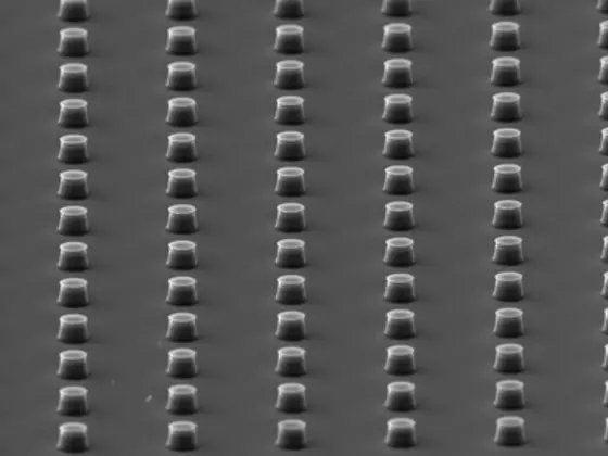
Silicon array pattern
Semiconductor
University cleanrooms and pilot lines run NineScrolls etch and deposition platforms across device R&D — from gate and contact patterning to dielectric stacks and surface preparation before bonding.
ICP-RIE and RIE systems cover anisotropic silicon and dielectric etching with controlled sidewall profiles; PECVD and ALD platforms deposit the dielectric and barrier films those devices are built from.
Electrical characterization closes the loop: wafer probe stations support device-level measurement from routine parametric checks to low-temperature studies.
Wide-bandgap material processing
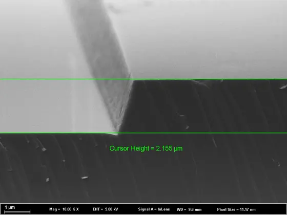
Diamond
Diamond and other wide-bandgap materials resist the etch chemistries that work for silicon; process development leans on high-density plasma sources and careful control of mask selectivity.
ICP-RIE platforms provide the ion energy and plasma density these hard-to-process materials demand, while HDP-CVD supports the dielectric films used in device stacks and hard masks.
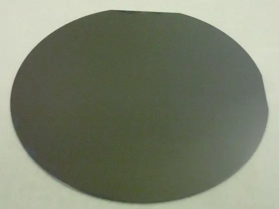
Four-inch SiO2 film deposition
Advanced Packaging
Wafer-level packaging research spans through-silicon vias, redistribution layers, and bonding surface preparation — each step depending on repeatable etch and deposition behavior.
PECVD platforms handle passivation and dielectric stacks; stripping systems clear resist between steps; plasma surface activation prepares wafers for bonding.
Silicon lens structure etch
MEMS
MEMS structures depend on deep, vertical silicon etches and clean release steps — the Bosch process alternates etch and passivation cycles to reach high aspect ratios without losing profile control.
RIE and ion-beam platforms cover the precision patterning and trimming steps around the deep etch, from device prototyping to failure analysis.
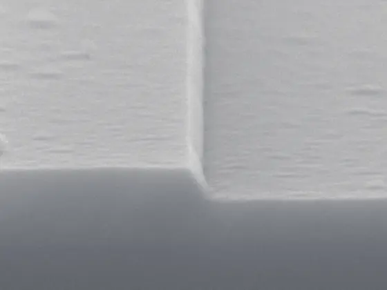
InP ridge structure etch
Photonics
Optical structures punish surface damage: ridge waveguides and photonic crystals need smooth, low-damage etches, and coating stacks need uniform, well-controlled films.
ICP-RIE platforms etch InP and related materials with the gentle ion energies photonics requires; wafer-level photonic test connects fabrication to measured device performance.
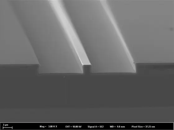
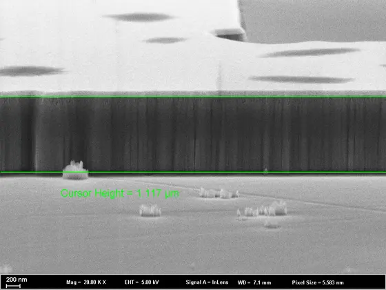
SiC etched profile
Power Electronics
SiC and GaN power devices bring hard-to-etch materials and demanding surface preparation into the process flow, with hard-mask schemes standing in for the photoresists that silicon processes rely on.
ICP-RIE covers the anisotropic etches; ALD deposits the conformal gate and passivation films that wide-bandgap device research depends on.
Next step
Map your application to a platform.
Tell us your material stack and process goals; a NineScrolls engineer will recommend a configuration.