Types of Wafer Probe Stations: Measurement-Environment Guide
By NineScrolls Engineering · 2026-07-20 · 14 min read · Metrology & Testing
TL;DR: six types, six buyer’s questions
Each probe-station type in this guide reduces to one buyer’s question — the single thing to put to a vendor before anything else on the datasheet:
- Standard ambient. Which upgrades will the platform accept later?
- Cryogenic. What does the stage deliver under your real heat load?
- High-temperature. How uniform and stable is the chuck across a long soak?
- Vacuum. Which signals must cross the chamber wall?
- RF & microwave. What does the daily calibration workflow look like?
- Silicon photonics. How repeatable is fiber-to-chip alignment?
One axis for the environment, one for the automation
Wafer probe stations are usually shopped by brand or by budget, but the taxonomy that actually predicts what a system can do for you is the measurement environment: the physical conditions the wafer sits in while the probes are landed. Room air on an open platen is one environment. A sealed chamber pumped free of atmosphere is another. A chuck held far above room temperature, a stage cooled deep below it, a signal path engineered for high-frequency work, an optical assembly that must hold a fiber over a grating coupler — each of these changes the hardware that surrounds the chuck, the specifications worth reading, and the cost structure of the system. The six types profiled below are six answers to the same underlying question: what must the station control around the device while you measure it?
The environment axis is deliberately orthogonal to the automation axis. Manual, semi-automatic, or fully automatic operation is a separate decision that composes with any environment, and the two should not be conflated: first fix the measurement environment, then fix the automation level. Environment determines what the platform must be physically built around and is expensive or impossible to retrofit; automation determines throughput and repeatability and is largely a platform option within a type. If you have not yet worked through the automation side, the decision framework in our probe-station selection guide covers it in depth; this article stays on the environment axis and does not repeat that material.
The six environment types
Every profile below follows the same five-part shape: what the type is and the hardware that distinguishes it, where it fits, what to review on a datasheet, what drives its cost, and when to walk away from it.
Standard ambient
The standard ambient station is the baseline the other five types are defined against: an open platen in room air, micropositioners around it, and an isolation table underneath. Nothing encloses the wafer — the environment is the lab itself. That simplicity is the point. Probes land quickly, chucks and positioners exchange freely, and the whole signal path is visible and reachable.
It is the right tool for general current–voltage and capacitance characterization, wafer-level debug, failure-analysis triage, and any teaching or multi-user facility where the sample mix changes weekly. On a datasheet, look past headline resolution claims to the architecture underneath: how the platen resists deflection when a probe arm is loaded, how positioner drift behaves across a long measurement, how the chuck holds planarity through its travel, and — most consequentially — which upgrades the platform will accept later. A thermal-chuck option, a shielded enclosure, added positioner stations: the upgrade paths available on the day of purchase define the system you will own years later. Cost concentrates in positioner precision and the isolation grade of the platform. A heavier, better-damped platform with finer positioners costs more and holds a contact more stably. For public price points and federal award examples across these configurations, see the worked examples in our selection guide.
Do not choose standard ambient when the measurement itself needs a controlled environment. Below-ambient work condenses moisture onto an open chuck, surface-sensitive samples degrade in room air, and no accessory retrofit turns an open platen into a sealed chamber. If your roadmap includes any of the five environments that follow, buy for that environment — or confirm the upgrade path in writing — rather than planning to grow out of an ambient platform.
Cryogenic
A cryogenic probe station replaces the open platen with a sealed, evacuated chamber and cools the sample stage with either a mechanical cryocooler or a liquid cryogen, with multi-stage vibration isolation placed between the cooling machinery and the probe contact. Every element of the baseline station is re-engineered: wiring becomes a heat path, viewing optics become a radiation path, and probe landing happens through a chamber rather than in open air.
It fits low-temperature device physics and the screening of superconducting and quantum devices — work whose signal only exists when the sample is cold. At survey level, the datasheet questions are all about honesty under load: what the stage actually delivers under your real heat load — probes landed, cables run, sample mounted — rather than on a bare stage; how vibration figures are stated, and in which cooler operating state they were taken; and how many signal lines can enter the chamber before the thermal budget is exceeded [1]. Cost concentrates in the cooling architecture, the number of isolation stages, and the radiation shielding, and the coldest configurations carry the steepest engineering cost.
This profile stays deliberately brief because the deep dive already exists: the cryogenic probe station buyer’s guide compares cooling architectures and builds an acceptance-ready RFQ, and the cryogenic probing application page covers when the environment is warranted at all. Do not choose cryogenic when a below-ambient thermal chuck would satisfy the physics — the chamber, the cooling plant, and the operating discipline are a cost worth carrying only when the measurement truly demands them.
High-temperature
A high-temperature station is built around a heated chuck sitting on a thermal-isolation stack. The engineering problem is not producing heat but containing it, so that the chuck surface runs hot while the positioners, the platen, and the optics above stay dimensionally stable. The visible hardware can look close to a standard ambient system; the difference is buried in the chuck construction and everything that isolates it.
It serves elevated-temperature device behavior and reliability studies: parameter drift with temperature, accelerated stress work, and the wide-bandgap programs — SiC and GaN power devices — whose operating regime is hot by design. On a datasheet, the numbers worth interrogating are architectural rather than headline: chuck uniformity across the plate and its stability across a long soak, thermal gradient control between the chuck surface and the positioner tips, and the leakage-current dynamics of the chuck’s isolation construction as temperature rises. Ask for the dielectric breakdown thresholds of thermal isolation stacks at operating temperature, not only at room temperature — an isolation figure quoted cold says little about the same stack hot. Wide-bandgap work adds a boundary condition of its own: power-device bias adds voltage stress on top of the thermal load, and thermal ratings and electrical ratings do not automatically compose — have the vendor state how the stack behaves under both stresses at once [3].
Cost concentrates in chuck uniformity engineering and in the thermal isolation of the positioners. Do not buy a dedicated high-temperature platform when the requirement is occasional, mild warming — a thermal-chuck option on an ambient platform covers that — and do not assume a heating-only system converts to below-ambient work later: heated and cooled chucks are different constructions, not settings on the same part.
Vacuum
A vacuum probe station encloses the chuck in a vacuum chamber, routes every signal through feedthrough wiring in the chamber wall, and lands probes with in-chamber probe arms driven from outside. The buyer’s question follows directly from the architecture — which signals must cross the chamber wall? Every crossing — electrical, mechanical, or optical — must be engineered, sealed, and rated; the chamber wall is where a vacuum configuration succeeds or fails.
It is suited to surface-sensitive devices, MEMS, and moisture-free measurement: released structures that stiction would destroy in humid air, films that oxidize between deposition and test, surfaces whose behavior shifts with adsorbed water. On a datasheet, review the chamber and pumping stack as one system — how the station reaches and holds its working pressure with the full wiring loom installed, how long a sample exchange takes from vent to measurement, and how feedthrough count and signal integrity hold up as channels are added; every extra line through the wall is a leak path and a noise path before it is a signal path [4]. Power-device work adds a boundary question: switching transients push brief current surges through the chamber wall, so ask for the transient current capacity of vacuum feedthroughs, not only their steady-state rating.
Cost concentrates in the chamber and pumping stack and in feedthrough count and signal integrity. Do not choose vacuum when dry is all you need — a purged enclosure on an ambient platform keeps moisture off most samples without a pump-down cycle — and remember that the chamber taxes every load: if the workflow lives on fast sample turnaround, vacuum will set its pace.
RF & microwave
An RF and microwave probe station is defined less by an enclosure than by its signal path: high-frequency positioners holding precision probes, a calibration-substrate holder in the chuck area, and low-loss cabling from probe tip to instrument. The station is one half of a measurement system whose other half is the network analyzer, and the two are joined by a calibration that must be renewed constantly.
It handles on-wafer high-frequency parameter extraction — characterizing transistors, passives, and interconnects in their high-frequency behavior rather than at quasi-static bias. On a datasheet, the headline frequency figure matters less than the workflow behind it: the transition-loss behavior of the probe-to-pad interface, the stability of the cabling as positioners move, the condition and lifetime of the probes themselves, and above all the daily calibration workflow — where the calibration substrate sits, how long a full calibration takes, how often probe wear forces one, and how the operator verifies that yesterday’s calibration still holds [2]. A station that makes calibration awkward produces data whose error grows quietly.
Cost concentrates in calibration substrates, low-loss interconnect, and the probe replacement cycle — RF probes are consumables, and their replacement rhythm belongs in the operating budget, not the surprise column. Do not choose an RF station for work that is genuinely quasi-static: the probes, the calibration overhead, and the operator discipline are wasted on measurements a general-purpose station handles. The reverse migration is no easier — adding high-frequency capability to an ambient platform later usually means new positioners, new cabling, and a calibration workflow designed from scratch.
Silicon photonics
A silicon photonics probe station adds an optical axis to the electrical one: fiber positioners with alignment optics hold single fibers or fiber arrays over grating couplers or against chip facets, alongside conventional electrical probes on the same die. The defining engineering problem is alignment — an optical coupling lives or dies on positioning tolerances far tighter than an electrical contact ever demands.
It is built for wafer-level optical coupling and photonic-circuit test: insertion measurements across a die map, wavelength response of ring and interferometer structures, and the combined electro-optic tests that photonic transceivers require. On a datasheet, everything reduces to the buyer’s question — how repeatable is fiber-to-chip alignment? Review how the alignment search runs and locks, how coupling holds during a measurement and through chuck motion between devices, how the system re-finds alignment on the next device of a die map, and how electrical probing and optical coupling coexist without disturbing each other [5]. The silicon photonics probing application page covers where wafer-level optical test earns its place in a photonics flow.
Cost concentrates in alignment automation and optical instrumentation integration — the difference between a manual alignment bench and an automated search-and-lock system is the difference between a demonstration and a test flow. Do not choose a photonic station for occasional coupling experiments; a bench setup couples one device at a time perfectly well. The station earns its cost when devices are counted in die maps rather than one-off samples.
The master comparison matrix
The same comparison, side by side. Read it column by column to place your measurement, then row by row to see what that placement costs and what to ask before quoting.
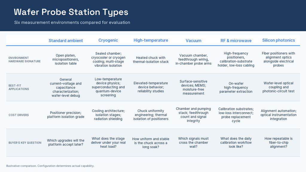
| Standard ambient | Cryogenic | High-temperature | Vacuum | RF & microwave | Silicon photonics | |
|---|---|---|---|---|---|---|
| Environment hardware signature | Open platen, micropositioners, isolation table | Sealed chamber; cryocooler or cryogen cooling; multi-stage vibration isolation | Heated chuck with thermal-isolation stack | Vacuum chamber, feedthrough wiring, in-chamber probe arms | High-frequency positioners, calibration-substrate holder, low-loss cabling | Fiber positioners with alignment optics alongside electrical probes |
| Best-fit applications | General current–voltage and capacitance characterization; wafer-level debug | Low-temperature device physics; superconducting and quantum-device screening | Elevated-temperature device behavior; reliability studies | Surface-sensitive devices; MEMS; moisture-free measurement | On-wafer high-frequency parameter extraction | Wafer-level optical coupling and photonic-circuit test |
| Cost drivers | Positioner precision; platform isolation grade | Cooling architecture; isolation stages; radiation shielding | Chuck uniformity engineering; thermal isolation of positioners | Chamber and pumping stack; feedthrough count and signal integrity | Calibration substrates; low-loss interconnect; probe replacement cycle | Alignment automation; optical instrumentation integration |
| Buyer’s key question | Which upgrades will the platform accept later? | What does the stage deliver under your real heat load? | How uniform and stable is the chuck across a long soak? | Which signals must cross the chamber wall? | What does the daily calibration workflow look like? | How repeatable is fiber-to-chip alignment? |
The type-selection checklist
Whichever type the roadmap points to, the same discipline applies when the request for quotation goes out. Ask every vendor to:
- Name the environment. Confirm in writing which measurement environment the quoted configuration is engineered for — and which it merely tolerates.
- Condition every claim. For each controlled-environment figure, state the load, the duration, and the operating state of the system when the figure was measured.
- Map the boundary crossings. List every signal that crosses the environment boundary — electrical, thermal, optical — and how each crossing is engineered and rated.
- Provide the upgrade map. Specify which chucks, positioners, enclosures, and signal options the platform accepts after purchase, and which require a different platform.
- Demonstrate the daily workflow. Show probe landing, calibration or alignment, and sample exchange as they would run in your lab, not as a brochure describes them.
- Itemize the consumables. State what the configuration consumes in operation — cryogens, calibration substrates, probe tips, pumping maintenance — and who supplies each.
- Rate combined stresses. For power-device work, state how isolation stacks and feedthroughs behave under electrical and thermal stress together, not as separate ratings.
If the purchase runs through institutional funding, our probe-station procurement guide pairs this checklist with the funding and compliance side of the purchase.
Where NineScrolls fits
Once the environment type is settled, the practical question becomes the procurement path. NineScrolls provides US and Canada procurement, import, and after-sales support for SEMISHARE wafer probe stations, quoting configurations against the acceptance criteria in the checklist above — the environment named, the claims conditioned, the crossings mapped. For the wider selection framework across automation level, sample size, and signal type, the wafer probe stations hub walks through the whole decision.
Further reading
This type map is one lane of the probe-station cluster. For the decision framework across automation level, sample size, and budget, read How to Choose a Wafer Probe Station for Your University Research Lab. For the compliance side of an institutional purchase, see the probe-station procurement guide for federally funded projects. And if the environment decision landed on cold, the cryogenic probe station buyer’s guide is the deep dive.
References
- NIST, "A Model for the Transient Behavior of a Pulse Tube Cryocooler" — separates no-load temperature, added thermal mass, net cooling capacity, and cooldown time — nist.gov/publications/model-transient-behavior-pulse-tube-cryocooler. Accessed 2026-07-19.
- R. B. Marks, "A multiline method of network analyzer calibration," IEEE Transactions on Microwave Theory and Techniques, vol. 39, no. 7, pp. 1205–1215, 1991 — the NIST multiline TRL method underlying modern on-wafer calibration practice.
- T. Kimoto and J. A. Cooper, Fundamentals of Silicon Carbide Technology: Growth, Characterization, Devices and Applications. Wiley-IEEE Press, 2014 — device physics and characterization context for SiC power-device testing.
- A. Chambers, Modern Vacuum Physics. Boca Raton: Chapman & Hall/CRC, 2004 — pumping, pressure measurement, and vacuum-chamber practice.
- L. Chrostowski and M. Hochberg, Silicon Photonics Design: From Devices to Systems. Cambridge University Press, 2015 — includes wafer-scale photonic test and fiber-to-chip coupling design.