Spin Coating & Development: A Complete Guide to Photoresist Processing
By NineScrolls Engineering · 2026-03-27 · 16 min read · Nanotechnology
Target Readers: Photolithography process engineers, cleanroom technicians, research scientists, lab managers, and technical decision-makers evaluating spin coating and development equipment. Newcomers will find the fundamentals and process flow sections valuable; experienced engineers can skip to the parameter optimization tables, troubleshooting guide, and photoresist selection chart.
TL;DR
- Spin coating produces uniform thin films (nm to hundreds of µm) by balancing centrifugal force, viscous flow, and solvent evaporation. Film thickness scales as ω−1/2 — doubling spin speed reduces thickness by ~30%.
- The full lithography flow is: substrate prep → spin coat → soft bake → expose → post-exposure bake (PEB) → develop → hard bake. Each step has critical parameters that affect the final pattern.
- Key parameters to control: spin speed (±1 rpm stability matters), acceleration ramp, dispense volume, bake temperature (±0.5°C), bake time, and ambient humidity (±5% RH).
- Development method (puddle vs spray), time, and temperature must be optimized together — underdevelopment leaves residue; overdevelopment erodes features and degrades CD control.
- Common defects (comets, striations, edge bead, poor adhesion) are almost always traceable to a specific process parameter — use the troubleshooting table in Section 7 for systematic diagnosis.
1) Spin Coating Fundamentals
Spin coating is the dominant method for depositing uniform thin films of photoresist, dielectrics, and other solution-processable materials onto flat substrates. The technique is elegantly simple: dispense a liquid onto a substrate, spin the substrate at high speed, and let centrifugal force and solvent evaporation produce a uniform film. Despite this simplicity, the underlying physics involves a rich interplay of fluid dynamics, rheology, and mass transport.
1.1 The Physics of Spin Coating
When a viscous liquid is placed on a spinning substrate, three forces compete:
- Centrifugal force — drives radial outflow, thinning the film. Scales with ω²r (angular velocity squared times radial position).
- Viscous resistance — opposes flow. Higher viscosity resists thinning and yields thicker films.
- Solvent evaporation — increases local viscosity as the film thins, eventually “freezing” the film at its final thickness. Evaporation rate depends on solvent vapor pressure, ambient temperature, and airflow above the substrate.
The spin coating process proceeds through four distinct phases:
- Deposition: Liquid is dispensed onto the substrate (static or dynamic dispense).
- Spin-up: The substrate accelerates to the target speed. During this phase, centrifugal force rapidly ejects excess liquid. The acceleration ramp rate determines how the initial fluid redistribution occurs.
- Spin-off: At constant speed, the film thins primarily through radial outflow. Excess liquid is flung off the substrate edge.
- Evaporation-dominated thinning: As the film becomes thin enough that viscous forces dominate centrifugal ejection, further thinning occurs primarily through solvent evaporation. This phase determines the final film thickness.
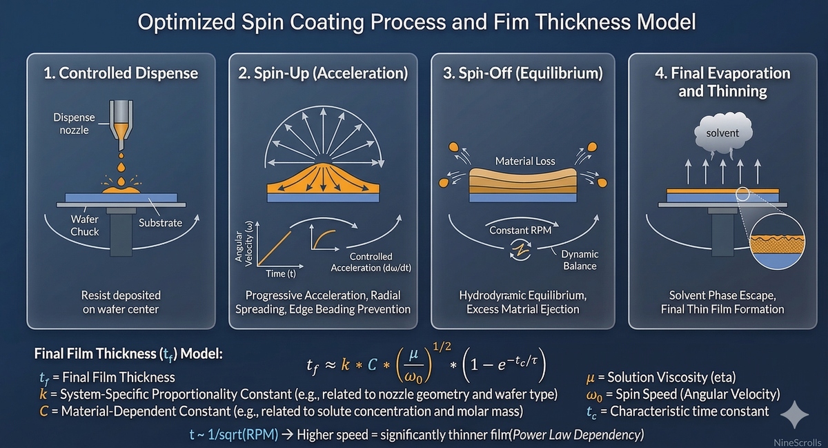
1.2 The Film Thickness Equation
The Meyerhofer model provides the foundational relationship for spin-coated film thickness:
t = k · Cβ · ηγ · ω−α
where t = film thickness, k = calibration constant, C = solution concentration (% solids), η = viscosity (cP), ω = angular velocity (rpm), and α ≈ 0.5, β ≈ 2, γ ≈ 0.33 for most resist systems.
The critical exponent is α ≈ 0.5, meaning film thickness scales as the inverse square root of spin speed. Practical implications:
- Doubling spin speed from 2000 to 4000 rpm reduces thickness by ~29% (factor of 1/√2).
- To halve the film thickness, you must quadruple the spin speed.
- Fine thickness adjustments (±5%) are more easily achieved by tuning solution concentration or viscosity than spin speed.
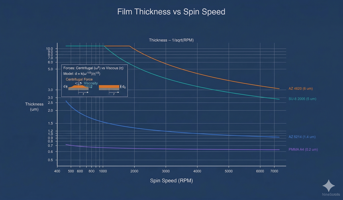
Most photoresist manufacturers provide spin speed vs thickness curves for their products. These empirically-derived curves are more accurate than the theoretical model because they account for specific solvent systems, polymer molecular weight distributions, and evaporation kinetics unique to each formulation.
1.3 Viscosity and Spin Speed Relationship
Understanding how viscosity interacts with spin speed is essential for process design:
| Viscosity Range (cP) | Typical Resist Type | Thickness Range | Spin Speed Range | Notes |
|---|---|---|---|---|
| 1–10 | Dilute PMMA, thin imaging layers | 50 nm – 500 nm | 2000–6000 rpm | Sensitive to humidity; dynamic dispense recommended |
| 10–100 | Standard positive resists (AZ, SPR) | 0.5–5 µm | 1000–5000 rpm | Most common regime; well-characterized spin curves available |
| 100–1000 | Thick resists (AZ 4620, SPR 220) | 5–30 µm | 500–3000 rpm | Multi-step spin profiles often needed; edge bead significant |
| 1000–50000+ | SU-8, thick KMPR, polyimide | 20–500+ µm | 500–3000 rpm | Slow ramp rates critical; extended soft bake required |
1.4 Coating Uniformity
Film thickness uniformity across the wafer is characterized by the 3σ variation (three standard deviations of thickness measured at multiple points). Key factors affecting uniformity include:
- Chuck flatness and vacuum: Non-uniform vacuum clamping causes local thickness variations. The chuck must hold the substrate perfectly flat.
- Acceleration profile: Abrupt acceleration can cause radial thickness gradients. A controlled ramp (typically 500–2000 rpm/s for standard resists) ensures smooth fluid redistribution.
- Dispense centering: Off-center dispense creates asymmetric thickness profiles. Automated dispense arms with positional accuracy of ±0.5 mm are preferred.
- Exhaust and airflow: Asymmetric exhaust causes one-sided evaporation, leading to thickness wedge patterns. Bowl exhaust should be symmetric and controlled.
- Environmental control: Temperature and humidity gradients across the substrate cause differential evaporation. Systems with environmental enclosures (23±0.5°C, 45±5% RH) achieve the best uniformity.
State-of-the-art spin coaters achieve <0.5% thickness uniformity (3σ) on 200 mm wafers with proper environmental control and optimized dispense/spin recipes.
2) The Lithography Process Flow
Spin coating and development are two steps in the larger photolithography process. Understanding the complete flow is essential because parameters at each step interact — an apparently good coat can produce poor results if bake or development conditions are wrong.
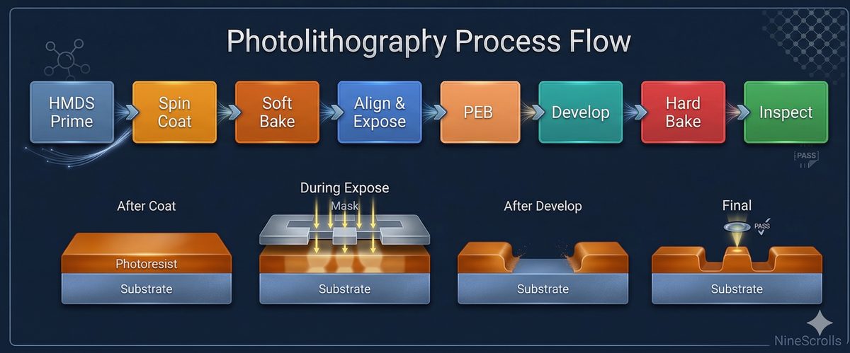
2.1 Substrate Preparation
Proper substrate preparation is the most frequently overlooked step in lithography, yet it has an outsized impact on pattern quality:
- Cleaning: Remove organic contaminants, particles, and native oxide. Common methods include piranha clean (H₂SO₄:H₂O₂), SC-1/SC-2 (RCA clean), solvent rinse (acetone → IPA → DI water), or O₂ plasma descum.
- Dehydration bake: Heat the substrate to 150–200°C for 5–10 minutes to remove adsorbed moisture. This step is critical — residual water on the substrate surface causes adhesion failure and resist popping during soft bake.
- Adhesion promoter: Apply hexamethyldisilazane (HMDS) via vapor prime (preferred) or liquid spin coat. HMDS converts surface hydroxyl groups (–OH) to trimethylsilyl groups (–Si(CH₃)₃), making the surface hydrophobic and dramatically improving resist adhesion. Vapor priming at 150°C in a vacuum oven produces the most reproducible results.
2.2 Spin Coating
The resist is dispensed and spun to the target thickness. A typical recipe consists of:
- Dispense step: 1–5 mL of resist dispensed at substrate center (static dispense at 0 rpm, or dynamic dispense at 500–800 rpm).
- Spread step: Ramp to 500–800 rpm at moderate acceleration (200–500 rpm/s) for 2–5 seconds to spread the resist across the substrate.
- Spin step: Ramp to final speed (1000–6000 rpm) at controlled acceleration (500–8000 rpm/s) and hold for 30–60 seconds.
- Deceleration: Controlled ramp-down to 0 rpm. Abrupt stops can cause resist reflow at the substrate edge.
For thick resists (>10 µm), multi-step profiles with intermediate hold speeds help avoid striations and improve uniformity. For very thin films (<200 nm), high spin speeds (4000–8000 rpm) with dynamic dispense minimize material waste.
2.3 Soft Bake (Pre-Bake)
The soft bake removes ~80–95% of the resist solvent, converting the liquid film to a solid. This step is essential for:
- Preventing the mask from sticking to the resist during contact/proximity exposure
- Reducing standing wave effects during exposure
- Establishing the correct resist chemistry for exposure and development
Hotplate baking is preferred over convection oven baking because heat transfers from the substrate up through the resist, allowing solvent to evaporate from the top surface without trapping bubbles. Typical conditions:
| Resist Type | Soft Bake Temp | Soft Bake Time | Notes |
|---|---|---|---|
| Standard positive (AZ 1500, SPR 700) | 90–100°C | 60–90 s | Hotplate; overbaking reduces sensitivity |
| Thick positive (AZ 4620, SPR 220) | 100–115°C | 2–5 min | Ramp slowly to avoid nitrogen bubbling; may require multi-step bake |
| SU-8 (negative epoxy) | 65°C → 95°C ramp | 3–30 min (thickness-dependent) | Two-step ramp critical; fast cooling causes stress cracking |
| PMMA (e-beam resist) | 170–180°C | 60–90 s | Higher bake temp than optical resists; improves resolution |
2.4 Exposure
UV light (or electron beam) transfers the mask pattern into the resist by triggering a photochemical reaction. The exposure dose (mJ/cm²) must be calibrated for the specific resist thickness, bake conditions, and development process. Under-exposure causes incomplete pattern transfer; over-exposure causes feature widening (positive resist) or feature narrowing (negative resist).
2.5 Post-Exposure Bake (PEB)
PEB is critical for chemically amplified resists (CARs) and SU-8, where it drives the acid-catalyzed crosslinking or deprotection reaction initiated by exposure. For conventional DNQ/novolac resists, PEB is optional but can reduce standing wave effects by allowing diffusion of the photoactive compound. Typical PEB temperatures are 5–15°C above the soft bake temperature, with tight uniformity (±0.5°C across the wafer) required for CD control.
2.6 Development
The developer selectively dissolves either the exposed (positive resist) or unexposed (negative resist) regions. Development is covered in detail in Section 6.
2.7 Hard Bake (Post-Bake)
A final bake at 110–150°C crosslinks the remaining resist, improving its resistance to subsequent etch or implant steps. Hard bake also drives off residual solvent and developer, improving adhesion. For resists that will be used as permanent structures (e.g., SU-8 MEMS), hard bake at 150–200°C provides maximum mechanical and chemical stability.
3) Key Process Parameters
Achieving reproducible lithography results requires precise control of multiple interacting parameters. This section quantifies the impact of each variable and provides practical control targets.
3.1 Spin Speed
Spin speed is the primary thickness control parameter. For production-grade results, speed stability of ±1 rpm is essential — speed fluctuations directly translate to thickness non-uniformity.
Rule of thumb: A 1% change in spin speed produces approximately a 0.5% change in film thickness (from the t ∝ ω−0.5 relationship). At 3000 rpm, a ±30 rpm variation causes ~±0.5% thickness variation — acceptable for most processes. At ±1 rpm control, thickness stability from spin speed alone is <0.02%.
3.2 Acceleration
The spin-up acceleration profile has a surprisingly large effect on coating quality:
- Low acceleration (100–500 rpm/s): Best for thick, high-viscosity resists. Allows gradual fluid redistribution and avoids radial striations. May leave spiral patterns if too slow.
- Medium acceleration (500–2000 rpm/s): Standard range for most positive photoresists. Good balance of uniformity and throughput.
- High acceleration (2000–8000 rpm/s): Used for thin films and low-viscosity resists where rapid spin-up minimizes material waste. Requires stable chuck vacuum to prevent substrate slip.
3.3 Dispense Volume and Method
Dispense volume affects material consumption, coating uniformity, and defect density:
| Substrate Size | Static Dispense Volume | Dynamic Dispense Volume | Savings with Dynamic |
|---|---|---|---|
| 2” (50 mm) | 1–2 mL | 0.5–1 mL | ~50% |
| 4” (100 mm) | 2–4 mL | 1–2 mL | ~50% |
| 6” (150 mm) | 3–6 mL | 1.5–3 mL | ~50% |
| 8” (200 mm) | 4–8 mL | 2–4 mL | ~50% |
| 12” (300 mm) | 5–10 mL | 2–5 mL | ~50% |
Dynamic dispense (dispensing onto a slowly spinning substrate at 500–800 rpm) reduces waste by approximately 50% compared to static dispense (dispensing onto a stationary substrate). Dynamic dispense also reduces the probability of trapped air bubbles under the resist puddle.
3.4 Bake Temperatures
Bake temperature uniformity is as important as the absolute temperature. A hotplate with ±0.5°C uniformity across the substrate is the minimum requirement for reproducible lithography.
- Soft bake under-temperature: Excess residual solvent causes mask contamination (contact lithography), resist tackiness, and irregular development.
- Soft bake over-temperature: Thermal decomposition of photoactive compound (PAC) reduces resist sensitivity and contrast. In extreme cases, the resist becomes insoluble in developer.
- PEB variation: For chemically amplified resists, a 1°C PEB error can shift the critical dimension (CD) by 5–10 nm. PEB uniformity is the most critical bake in advanced lithography.
3.5 Humidity and Environment
Ambient conditions during coating and baking have a measurable impact on lithographic performance:
- Humidity during coating: High humidity (>55% RH) causes water absorption into the resist film during spinning, leading to haze, reduced adhesion, and variable development rates. Low humidity (<30% RH) accelerates solvent evaporation, causing premature skin formation and radial thickness gradients.
- Temperature during coating: Resist viscosity is temperature-dependent (−25% per 10°C for typical solvents). Uncontrolled ambient temperature causes run-to-run thickness variation.
- Optimal conditions: Environmental enclosures maintaining 23±0.5°C and 45±5% RH provide the best reproducibility for critical lithography.
4) Photoresist Selection Guide
Selecting the right photoresist for your application requires balancing resolution, thickness range, process compatibility, and cost. The following table compares the most commonly used photoresists across research and production environments:
| Resist | Tone | Chemistry | Resolution | Thickness Range | Developer | Key Applications |
|---|---|---|---|---|---|---|
| AZ 1500 series | Positive | DNQ/novolac | 0.5–1 µm | 0.5–2.5 µm | AZ 300 MIF (2.38% TMAH) | General photolithography, contact/proximity |
| AZ 4620 | Positive | DNQ/novolac | 3–5 µm | 6–25 µm | AZ 400K (diluted KOH) | MEMS, deep etch masks, electroplating molds |
| SPR 220 | Positive | DNQ/novolac | 2–4 µm | 3–30 µm | MF-26A (2.38% TMAH) | Thick resist lithography, MEMS, TSV |
| SU-8 | Negative | Epoxy (CAR) | 1–2 µm | 1–500+ µm | SU-8 Developer (PGMEA) | MEMS structures, microfluidics, permanent dielectric |
| PMMA | Positive | Chain scission | <10 nm (e-beam) | 50 nm – 2 µm | MIBK:IPA (1:3) | E-beam lithography, nanoimprint, lift-off |
| AZ nLOF 2000 series | Negative | DNQ-based image reversal | 0.5–1 µm | 1–15 µm | AZ 300 MIF (2.38% TMAH) | Metal lift-off (undercut profile) |
| ma-N 1400 series | Negative | Crosslinking | 0.5–1 µm | 0.5–3 µm | ma-D 533/S (TMAH-based) | High-resolution negative patterning, wet etch masks |
| AZ 5214E | Pos/Neg (image reversal) | DNQ/novolac + crosslinker | 0.8–1.5 µm | 0.5–2 µm | AZ 300 MIF (2.38% TMAH) | Metal lift-off, image reversal for undercut |
Positive vs Negative Resists: When to Use Each
- Positive resists (exposed regions dissolve): Preferred for most patterning because they offer higher resolution, better CD control, and straightforward processing. Use for etch masking, implant masking, and general photolithography.
- Negative resists (exposed regions remain): Preferred for lift-off processes (undercut profile is inherent), thick permanent structures (SU-8), and applications where the remaining resist area is smaller than the removed area (reduces development time). Watch for swelling-induced resolution limits in conventional negative resists.
- Image reversal resists (AZ 5214E): Offer the best of both worlds — can be used as either positive or negative. In image reversal mode, they provide undercut profiles ideal for metal lift-off while maintaining the high resolution of a positive resist.
5) Development Process Optimization
Development is the pattern-defining step of lithography. The developer selectively dissolves resist to reveal the desired pattern. Poor development control is one of the most common causes of lithographic failure, yet it receives less attention than exposure optimization in many labs.
5.1 Development Methods
| Method | Description | Advantages | Disadvantages | Best For |
|---|---|---|---|---|
| Puddle (static) | Dispense developer to cover wafer surface; hold static for timed interval; spin rinse with DI water | Low developer consumption; gentle (minimal pattern erosion); excellent uniformity with proper puddle formation | Slower; dissolved resist products can redeposit if puddle is held too long | Thin resists, high-resolution patterns, CD-critical layers |
| Spray | Spray fresh developer onto spinning wafer through a nozzle | Faster; continuous fresh developer supply; better at clearing high-aspect-ratio features | Higher developer consumption; more aggressive (can erode thin features) | Thick resists, high-aspect-ratio features, production throughput |
| Multi-puddle | Sequential puddle–rinse–puddle cycles (typically 2–3 cycles) | Combines gentleness of puddle with fresh developer supply; minimizes redeposition | Longer cycle time; more complex recipe programming | Thick resists where single puddle leaves residue; high-AR features |
| Immersion | Submerge wafer in developer bath with agitation | Simple; good for batch processing small substrates | Developer becomes loaded with dissolved resist; poor uniformity; not recommended for production | R&D with small pieces; SU-8 development (long soak times) |
5.2 Development Time Optimization
The optimal development time is a balance between complete pattern clearing and minimizing resist erosion:
- Underdevelopment: Leaves thin resist residue (“scum”) in developed regions. This residue blocks subsequent etch or deposition, causing pattern defects. Often manifests as a translucent film visible under inspection microscope.
- Overdevelopment: Erodes feature sidewalls, widens trenches (positive resist), narrows lines (positive resist), and reduces resist thickness. Also causes “footing” (resist residue at the substrate interface) to become more pronounced in some systems.
- The development window: For a well-optimized process, the development window should be at least ±15% of the nominal development time. If the window is narrower, adjust the exposure dose or soft bake to improve resist contrast.
Practical tip: Use the “10% over-development” rule as a starting point. If your nominal development time is 60 seconds, develop for 66 seconds. This small margin ensures complete clearing without significant feature erosion. Verify the exact margin needed for your specific resist/developer system through a development time matrix (expose a test wafer, cleave into strips, develop each strip for a different time).
5.3 Developer Temperature Control
Development rate is strongly temperature-dependent. For TMAH-based developers, a 1°C increase in developer temperature increases the development rate by approximately 5–10%. This means:
- Developer temperature should be controlled to ±0.5°C for reproducible CD control.
- If developer is stored at room temperature and room temperature varies by ±2°C, development rate can vary by ±10–20% — a significant source of process variability.
- For critical processes, use a developer temperature control module or ensure the developer is equilibrated to the process temperature before dispense.
5.4 Rinse and Dry
After development, a thorough DI water rinse (10–30 seconds at 300–500 rpm) quenches the development reaction and removes dissolved resist products. Follow with a high-speed spin dry (2000–5000 rpm for 15–30 seconds). For high-aspect-ratio features, a brief IPA rinse before spin dry reduces pattern collapse caused by surface tension (Marangoni effect).
6) Troubleshooting Common Issues
This section provides a systematic guide to diagnosing and resolving the most common spin coating and development defects. Each defect is traced to its root cause with specific corrective actions.
| Defect | Appearance | Root Causes | Corrective Actions |
|---|---|---|---|
| Comets | Radial streaks originating from particles, usually visible as tails pointing outward from a defect source | Particles on substrate or in resist; clogged dispense filter; contaminated resist bottle | Improve substrate cleaning; install/replace 0.2 µm inline dispense filter; filter or replace resist; clean dispense lines |
| Striations | Radial or spiral thickness variations visible as color fringes under sodium lamp or thin-film interference | Excessive acceleration for resist viscosity; premature resist drying during spread; low humidity; resist dispensed too far from center | Reduce acceleration; use dynamic dispense; increase ambient humidity (target 40–50% RH); ensure centered dispense; increase dispense volume |
| Edge bead | Thick resist ridge (5–20× nominal thickness) at the substrate edge, extending 1–5 mm inward | Surface tension causes resist to accumulate at the edge during spin-off; worse with thick, viscous resists | Use edge bead removal (EBR): dispense solvent at wafer edge during a dedicated EBR spin step; increase final spin speed; program a brief high-speed burst at the end of the spin recipe |
| Poor adhesion / delamination | Resist lifts or peels from substrate during development; visible as pattern distortion, missing features, or “flag” defects | Inadequate substrate cleaning; missing HMDS; insufficient dehydration bake; over-development; developer temperature too high | Add or improve HMDS vapor prime; increase dehydration bake time/temperature; verify substrate cleanliness; reduce development time or developer concentration |
| Incomplete development (scum) | Thin resist residue remaining in areas that should be fully cleared; may be invisible to the eye but detectable by profilometer or etch test | Under-exposure; insufficient development time; developer depletion (immersion method); soft bake temperature too low (excess solvent inhibits dissolution) | Increase exposure dose; extend development time; use multi-puddle development; increase soft bake temperature; verify developer concentration/freshness |
| Bubbles / pinholes | Circular voids in the resist film, visible as bright spots under microscope; may be isolated or clustered | Nitrogen outgassing during soft bake (thick resists); air trapped during dispense; contaminated substrate surface; resist degassed improperly | Use slower soft bake ramp (1–2°C/min for thick resists); ensure dynamic dispense; degas resist before use; improve substrate cleaning |
| Standing waves | Periodic undulations in resist sidewall (visible as “scalloped” profile in SEM cross-section); period equals λ/(2n) where n is resist refractive index | Constructive/destructive interference of incident and reflected exposure light within the resist film | Apply bottom anti-reflective coating (BARC); use PEB to diffuse photoproducts and smooth the standing wave pattern; adjust resist thickness to a half-wave condition |
| Pattern collapse | High-aspect-ratio resist features bend or collapse during rinse/dry, often sticking to adjacent features | Capillary forces during drying exceed mechanical strength of resist features; aspect ratio (height:width) >3:1 at risk | Use IPA rinse before spin dry; reduce feature aspect ratio; use supercritical CO₂ drying for extreme AR; increase hard bake to strengthen resist |
| Thickness non-uniformity | Center-to-edge thickness gradient; visible as color variation across wafer | Asymmetric exhaust; off-center dispense; non-uniform chuck vacuum; temperature/humidity gradient; substrate not flat on chuck | Verify centered dispense; check chuck vacuum uniformity; ensure symmetric exhaust; control environment; verify substrate flatness |
7) Equipment Selection Guide
The right coater/developer system can mean the difference between reproducible, high-quality lithography and constant process troubleshooting. When evaluating equipment, consider the following critical specifications:
7.1 Spin Performance
- Speed range: Ensure the coater covers your required range. For standard photolithography, 0–6000 rpm is typical. For thin film coatings, you may need up to 8000 rpm. For thick resists, low-speed capability (<500 rpm with good stability) is important.
- Speed accuracy: ±1 rpm closed-loop control is the benchmark for production-grade equipment. Open-loop systems with ±10–50 rpm variation introduce unacceptable thickness variability.
- Acceleration: Programmable acceleration up to 8000 rpm/s enables recipe optimization for any resist viscosity. Step-wise acceleration profiles are essential for thick resist processing.
7.2 Hotplate Performance
- Temperature range: RT to 200°C covers all standard resist bakes. Higher temperature capability (up to 300°C+) is needed for polyimide curing and some permanent resist processes.
- Uniformity: ±0.5°C across the substrate is the minimum for reproducible lithography. Verify this specification at your operating temperature, not just at room temperature.
- Temperature stability: Fast PID control with minimal overshoot ensures consistent bake conditions from wafer to wafer.
7.3 Dispense System
- Number of lines: Minimum two photoresist lines (for different resist types or viscosities) on the coater module, plus two developer lines and a DI water rinse line on the developer module.
- Filtration: Inline 0.2 µm point-of-use filters on all resist lines eliminate particle-induced defects.
- Dispense accuracy: Syringe pump or pressurized dispense with ±2% volume repeatability ensures consistent film thickness.
7.4 Substrate Compatibility
Verify the system accommodates your substrate formats:
- Wafer sizes: 2” through 12” with appropriate vacuum chucks for each size.
- Non-standard substrates: Square substrates, small pieces, and irregularly shaped samples require adaptable chuck designs or custom carriers.
- Material compatibility: Ensure chemical compatibility of all wetted parts (bowl, drain, dispense lines) with your solvents, resists, and developers.
7.5 Environmental Control
For critical lithography, an environmental enclosure maintaining 23±0.5°C and 45±5% RH is essential. This option significantly improves run-to-run reproducibility and eliminates a major source of process variability — especially in facilities without centralized cleanroom HVAC control.
7.6 Automation and Programmability
- Recipe storage: Programmable multi-step profiles with stored recipes for different resist/substrate combinations enable rapid process changeover.
- Automated cleaning: Built-in solvent flush and bowl wash routines reduce cross-contamination and manual cleaning time.
- Edge bead removal (EBR): Programmable EBR with solvent dispense at the wafer edge eliminates the thick resist ridge that causes proximity gap issues in contact lithography and non-uniform edge exposure.
7.7 Modular Configuration
A modular coater/developer platform allows you to configure the system for your specific workflow — coating-only, development-only, or integrated coat-bake-develop in a single footprint. This flexibility is valuable for research environments where process requirements evolve over time.
8) Frequently Asked Questions
What spin speed should I use for a 1 µm thick photoresist film?
The required spin speed depends on the specific resist and its viscosity. As a rough guide, standard positive resists (AZ 1512, SPR 700) typically achieve 1 µm at 3000–4000 rpm. However, always consult the manufacturer’s spin speed vs thickness curve for your specific resist product — these curves are empirically derived and account for solvent system, molecular weight, and formulation-specific behavior. Start with the manufacturer’s recommended speed and fine-tune with profilometer measurements on test wafers.
How do I choose between puddle and spray development?
Use puddle development for thin resists (<5 µm), critical CD layers, and processes where minimal feature erosion is important. Use spray development for thick resists (>10 µm), high-aspect-ratio features that need aggressive developer penetration, and production environments where throughput matters. For thick resists in the 5–15 µm range, a multi-puddle approach (2–3 puddle cycles with intermediate DI rinse) often gives the best balance of clearing and CD control.
Why is my resist film thickness not matching the manufacturer’s spin curve?
Several factors can cause deviation from published spin curves: (1) Temperature: the spin curve was likely generated at 23°C — if your lab is warmer, resist viscosity is lower and the film will be thinner. (2) Humidity: high humidity causes water absorption that changes solvent evaporation dynamics. (3) Resist age: solvent evaporation from partially filled bottles increases viscosity over time, yielding thicker films. (4) Acceleration: different ramp rates change the amount of resist ejected during spin-up. (5) Exhaust conditions: strong exhaust accelerates solvent evaporation, increasing effective viscosity. Always characterize the spin curve on your specific equipment under your cleanroom conditions.
How important is HMDS for photoresist adhesion?
HMDS is critical for resist adhesion on silicon, SiO₂, and silicon nitride surfaces. Without HMDS, water molecules on the hydrophilic substrate surface create a weak boundary layer that causes resist delamination during development — especially in aqueous (TMAH) developers. Vapor-phase HMDS priming at 150°C is more effective and reproducible than liquid HMDS applied by spin coating. In our experience, the majority of “poor adhesion” complaints from lithography engineers are resolved by adding or improving the HMDS priming step.
Can I coat non-round substrates (square pieces, irregular samples)?
Yes, but with caveats. Non-round substrates create asymmetric airflow during spinning, which can cause thickness non-uniformity — particularly at the corners of square substrates. To mitigate this: (1) use a carrier wafer with the sample mounted at center using vacuum or thermal release tape; (2) increase the dispense volume to ensure full coverage; (3) reduce spin speed (the corners of a square experience higher effective velocity than the edges of a round wafer at the same RPM); (4) use an environmental enclosure to minimize airflow-induced evaporation asymmetry. Modern spin coaters with programmable chuck configurations can accommodate substrates from small pieces to 12” wafers and square substrates with appropriate fixturing.
What causes “comet” defects and how do I eliminate them?
Comets are caused by particles on the substrate surface or in the resist that act as nucleation points for thickness discontinuities during spinning. The centrifugal force drags resist away from the particle, creating a radial streak. Elimination strategy: (1) improve substrate cleaning (add O₂ plasma descum or an additional solvent rinse); (2) install or replace the inline point-of-use resist filter (0.2 µm); (3) purge the dispense line with several mL of resist before coating (the first dispense from a line often contains particles); (4) check resist bottle age and storage conditions — expired or improperly stored resist develops particle precipitates; (5) ensure the spin bowl is clean and free of dried resist that could flake onto the substrate.
How do I handle edge bead for thick resist processes?
Edge bead is inherent to spin coating and becomes progressively worse with increasing resist viscosity and thickness. For thick resists (>10 µm), the edge bead can be 50–100+ µm tall and extend 3–5 mm from the wafer edge. Solutions: (1) Edge bead removal (EBR): program a dedicated EBR step where solvent (typically PGMEA or EBR solvent) is dispensed at the wafer edge while spinning at moderate speed (500–1000 rpm). The solvent dissolves the excess resist at the edge. (2) Backside rinse: dispense solvent on the wafer backside during spinning to remove resist that wraps around the edge. (3) Optimize spin profile: a brief high-speed burst (e.g., 5000–8000 rpm for 2–3 seconds) at the end of the spin recipe ejects additional edge material. EBR is the most effective and reproducible method for edge bead control.
Do I need environmental control for my spin coater?
It depends on your process requirements. For R&D with relaxed CD tolerances (±0.5 µm), a cleanroom with standard HVAC (±2°C, ±10% RH) may be sufficient. For production lithography or any process where run-to-run thickness repeatability of <1% (3σ) is required, environmental control (23±0.5°C, 45±5% RH) is essential. The cost of an environmental enclosure is small compared to the cost of diagnosing and reworking yield losses caused by uncontrolled ambient conditions. If you are seeing unexplained day-to-day or season-to-season variation in your lithographic results, environmental control should be one of the first process improvements to investigate.
NineScrolls Coater/Developer Systems
Our coater/developer platform offers up to 8000 rpm spin speed with ±1 rpm accuracy, integrated hotplate with precise temperature distribution, modular coat/develop/bake configuration, optional environmental control (23±0.5°C, 45±5% RH), and programmable edge bead removal — everything you need for reproducible photolithography from R&D to production.