Plasma Stripping & Ashing – Principles, Gas Chemistry, and Equipment Guide
By NineScrolls Engineering · 2026-03-27 · 14 min read · Materials Science
Target Readers: Process engineers, equipment engineers, PIs/lab managers, R&D procurement teams, and technical decision-makers evaluating photoresist stripping and plasma ashing solutions. Newcomers will find the fundamentals and comparison tables helpful; experienced engineers can skip to the gas chemistry selection and process optimization sections.
TL;DR Summary
Plasma stripping (ashing) uses oxygen-based plasmas to convert organic films — photoresist, PMMA, polymer residues — into volatile CO₂ and H₂O, providing a dry, damage-controllable alternative to wet chemical stripping. By selecting the right gas chemistry (O₂, O₂/N₂, O₂/CF₄, or H₂/N₂), tuning RF power, pressure, temperature, and gas flow, engineers can strip photoresist at rates exceeding 1 µm/min while preserving sensitive substrates and metal interconnects. Beyond traditional PR removal, modern plasma strippers handle post-etch residue cleaning, descum, surface activation for bonding, organic contamination removal, and even selective etching of 2D materials (MoS₂, BN, graphene). This guide covers the underlying plasma chemistry, compares dry vs. wet stripping, provides gas-selection decision guidance, discusses special 2D material applications, and offers a full FAQ — everything needed to select, optimize, and run a plasma stripping process.
1) What Is Plasma Stripping / Ashing?
Plasma stripping — also called plasma ashing — is a dry-process technique that uses a low-pressure, RF-generated plasma to remove organic materials from a substrate surface. The most common application is photoresist removal after lithographic patterning and etching, but the technique extends to any scenario requiring controlled removal of organic films.
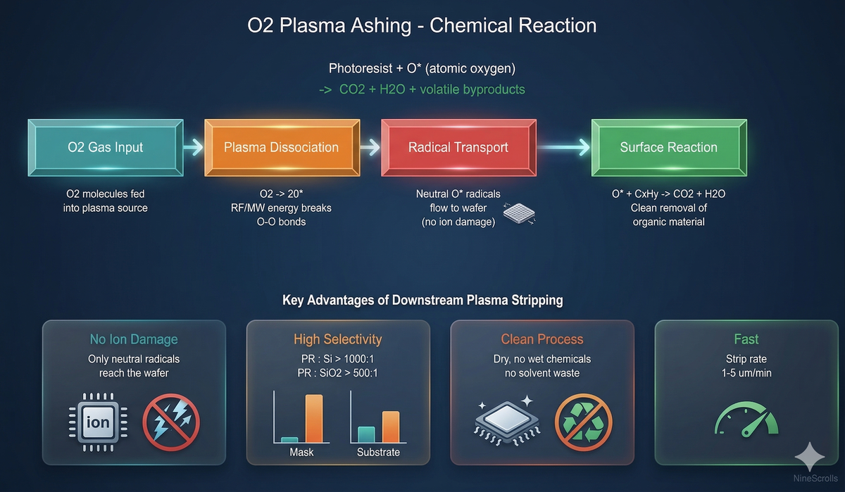
1.1 The O₂ Plasma Chemistry
In a typical oxygen plasma, the 13.56 MHz RF field dissociates O₂ molecules into a mixture of reactive species:
- Atomic oxygen radicals (O*): The primary etchant — these neutral, highly reactive species attack C–C and C–H bonds in organic materials
- Ozone (O₃): A secondary oxidant that contributes to organic decomposition
- O₂⁺ ions: Provide directional bombardment energy when accelerated across the plasma sheath
- UV photons: Break polymer chains through photo-dissociation, increasing surface reactivity
- Metastable O₂*: Excited-state molecules that transfer energy to surface species on contact
The fundamental stripping reactions for a generic hydrocarbon photoresist (CₓHᵧOᵤ) are:
- C + 2O* → CO₂↑ (primary carbon removal pathway)
- C + O* → CO↑ (secondary pathway, favored at low O* concentration)
- 2H + O* → H₂O↑ (hydrogen removal)
- CₓHᵧ + (2x + y/2) O* → xCO₂↑ + (y/2) H₂O↑ (net reaction)
All reaction products (CO₂, CO, H₂O) are gases at process conditions and are continuously pumped away, leaving a clean, residue-free surface. This self-cleaning characteristic is a major advantage over wet stripping, where dissolved resist can re-deposit.
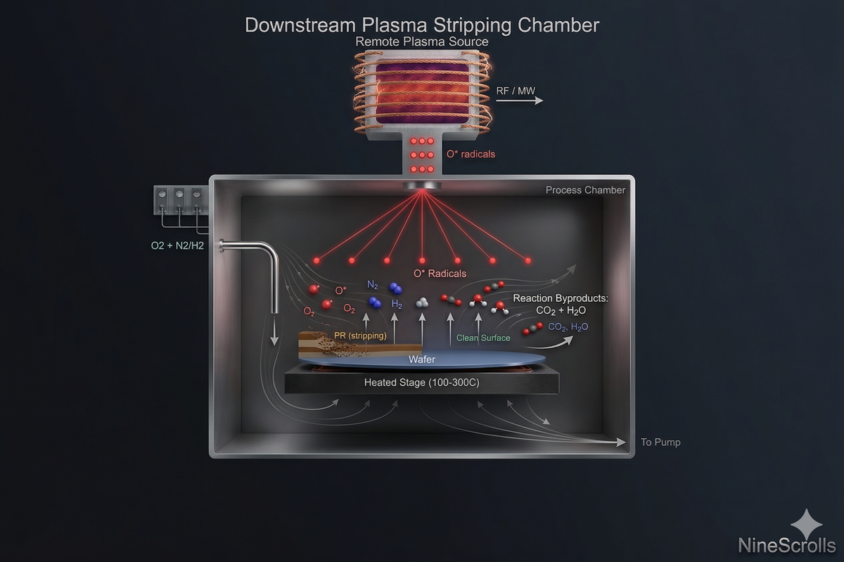
1.2 Downstream vs. Direct Plasma Configurations
Plasma strippers operate in two main configurations:
- Direct plasma (in-situ): The wafer sits within or directly adjacent to the plasma discharge zone. Both radicals and ions reach the substrate, providing high strip rates (1–5 µm/min) but with more ion bombardment. Suitable for robust substrates and when speed is paramount.
- Downstream (remote) plasma: The plasma is generated upstream and only neutral radicals flow to the wafer. Ion bombardment is minimal, making this configuration ideal for damage-sensitive substrates (III-V compounds, MEMS devices, thin gate oxides). Strip rates are lower (0.3–2 µm/min) but controllability and gentleness are superior.
NineScrolls Striper systems use an adjustable plasma discharge gap that allows operators to tune the balance between direct and downstream exposure — effectively providing both configurations in a single platform.
1.3 Why "Ashing"?
The term "ashing" comes from the analogy to combustion: organic material is oxidized to gaseous products, leaving behind only inorganic residue (the "ash"). In semiconductor processing, this ash consists of metal oxides, ion-implant residues, or inorganic filler particles from the photoresist formulation. A complete strip process often includes an ashing step followed by a residue removal step to handle this inorganic remnant.
2) Plasma Stripping vs. Wet Chemical Stripping
Both plasma (dry) and wet chemical methods can remove photoresist, but they differ significantly in mechanism, performance, and environmental impact. The following table provides a detailed comparison:
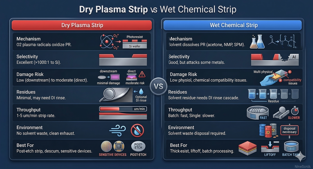
| Parameter | Plasma Stripping (Dry) | Wet Chemical Stripping |
|---|---|---|
| Mechanism | Radical oxidation + ion-assisted desorption | Chemical dissolution (solvents, acids, or oxidizers) |
| Common Chemistries | O₂, O₂/N₂, O₂/CF₄, H₂/N₂ | Piranha (H₂SO₄/H₂O₂), NMP, DMSO, EKC series |
| Strip Rate | 0.5–5 µm/min (tunable via power/pressure) | 0.1–2 µm/min (temperature-dependent) |
| Hardened / Ion-Implanted Resist | Effective — UV-hardened crust broken by ion bombardment + O* penetration | Difficult — crust blocks solvent penetration; requires multi-step processes |
| Uniformity | Excellent with center pump-down and tuned gas distribution (<5% non-uniformity) | Good with agitation; edge effects in batch tanks |
| Metal Compatibility | O₂ plasma can oxidize Cu, Ti, TiN — use H₂/N₂ for metal-sensitive layers | Solvent-based strippers generally metal-safe; Piranha attacks Cu |
| Substrate Damage | Controllable via power, pressure, and discharge gap; downstream mode minimizes damage | Minimal physical damage; chemical attack on sensitive films possible |
| Environmental / Safety | No liquid waste; exhaust scrubbed; small footprint | Large volumes of hazardous waste (acids, solvents); fume hoods required |
| Throughput | Single-wafer: 20–40 wph; multi-wafer batch: 50–100+ wph | Batch immersion: 50–200 wph (but long soak times) |
| Cost of Ownership | Higher equipment cost; low consumable cost (gases only) | Lower equipment cost; high consumable and waste disposal costs |
| Best Use Cases | Post-etch strip, hardened resist, controlled surface activation, 2D materials | Thick resist removal (>20 µm), lift-off processes, low-volume labs |
When to choose plasma stripping: Post-etch residue removal, ion-implanted resist, surface activation, descum, or any process requiring precise uniformity control and minimal chemical waste. Plasma stripping is also the only viable option for many 2D material processing applications where wet chemistries would destroy the monolayer films.
When to choose wet stripping: Very thick resist layers (>20 µm), lift-off processes where partial resist dissolution is needed, or when the substrate cannot tolerate any ion bombardment or UV exposure.
3) Key Process Types
3.1 Standard Photoresist Stripping
The most common application of plasma ashing is removal of positive-tone photoresist (e.g., DNQ/novolac i-line resists, chemically amplified DUV resists) after pattern transfer. A typical process flow:
- Pre-heat: Ramp wafer stage to target temperature (80–150 °C for standard PR; lower for temperature-sensitive substrates)
- Pump-down: Evacuate chamber to base pressure (<50 mTorr)
- Gas stabilization: Introduce O₂ at target flow rate (50–200 sccm); stabilize pressure (200–800 mTorr)
- Plasma ignition: Apply RF power (300–600 W); confirm stable plasma via reflected power reading
- Strip: Continue until endpoint detection signals resist clearance (typically 30–120 s for 1–2 µm thick resist)
- Over-ash: Continue for 10–30% additional time to ensure complete removal, especially in via and trench features
- Pump/purge: Evacuate reaction products; optional N₂ purge to remove residual O*
Process window for 1.5 µm i-line resist on Si: O₂ 100 sccm, 500 mTorr, 400 W, 120 °C stage temperature, strip rate ~2.5 µm/min, total process time ~60 s.
3.2 Post-Etch Residue Removal
After RIE or ICP-RIE etching, sidewall polymer deposits and redeposited etch by-products form residues that are not pure organic. These residues contain metal halides (from etched metal layers), silicon-containing polymers (from fluorocarbon passivation), and cross-linked photoresist (hardened by ion bombardment and UV exposure during etching).
Removing these residues requires more aggressive chemistry than standard PR stripping:
- O₂/CF₄ (95:5 to 90:10): The CF₄ additive generates fluorine radicals that attack Si-containing residues while O₂ handles the organic component. Etch selectivity to underlying SiO₂ must be monitored.
- O₂/N₂ (80:20): N₂ addition increases ion bombardment energy (heavier N₂⁺ ions) without introducing halogen species. Effective for moderate post-etch residues.
- Two-step process: (1) High-power O₂ to remove bulk organic, then (2) O₂/CF₄ at lower power to gently remove inorganic residue without attacking the underlying film stack.
3.3 Descum
Descum is a brief, low-power O₂ plasma treatment applied after photoresist development to remove thin organic residues (scum) from nominally cleared areas. These residues — typically 5–50 nm thick — result from incomplete development and can cause pattern transfer defects during subsequent etching.
Descum parameters are deliberately gentle:
- Power: 100–300 W (low to avoid resist erosion)
- Pressure: 200–500 mTorr
- Time: 10–30 seconds
- Temperature: Room temperature to 50 °C
The critical requirement is that descum removes scum without measurably thinning the patterned resist or altering its sidewall profile. For a 1 µm thick resist, a well-tuned descum process removes <20 nm of resist thickness while clearing scum completely.
3.4 Surface Activation
O₂ plasma exposure converts hydrophobic surfaces to hydrophilic by replacing surface C–H groups with polar C=O, C–OH, and COOH functionalities. This dramatically increases surface energy and is used for:
- Wafer bonding: Plasma-activated SiO₂ surfaces achieve bond energies >2 J/m² at room temperature, enabling direct bonding without adhesives
- Adhesion promotion: Improving metal or dielectric film adhesion to polymer substrates (e.g., PDMS, PI, PET)
- Wettability control: Ensuring uniform photoresist coating on hydrophobic surfaces
- Bio-functionalization: Creating reactive surface groups for biomolecule attachment in MEMS/microfluidics
Surface activation parameters are typically low power (100–300 W), low pressure (200–500 mTorr), and short duration (10–60 s). The activated surface has a limited lifetime — hydrophobic recovery begins within minutes to hours depending on the material — so subsequent processing should follow promptly.
3.5 2D Materials Processing
Plasma stripping finds a growing role in 2D materials research, where controlled removal of mask layers and selective etching of atomically thin films requires exceptional process control. This application is discussed in detail in Section 7.
4) Gas Chemistry Selection
The choice of process gas is the most impactful decision in plasma stripping. Each chemistry offers distinct advantages and limitations:
4.1 Pure O₂
The workhorse chemistry for standard photoresist stripping. O₂ plasma generates abundant atomic oxygen radicals that efficiently oxidize organic materials to volatile CO₂ and H₂O.
- Advantages: High strip rate, clean by-products, no halogen contamination, simple single-gas process
- Limitations: Oxidizes metal surfaces (Cu, Ti, TiN, W); cannot remove inorganic residues; may cause substrate oxidation damage
- Typical conditions: 100–200 sccm, 300–800 mTorr, 300–600 W
4.2 O₂/N₂ Mixtures
Adding 10–30% N₂ to O₂ increases the mean ion mass, enhancing physical sputtering of stubborn residues without introducing halogen contamination. N₂ also dilutes the O* radical density, providing a way to reduce strip rate for better endpoint control on thin resists.
- Advantages: Better post-etch residue removal than pure O₂; no fluorine contamination; improved uniformity at lower pressures
- Limitations: Still oxidizes metals; strip rate lower than pure O₂
- Typical conditions: O₂ 80 sccm + N₂ 20 sccm, 300–600 mTorr, 400–600 W
4.3 O₂/CF₄ Mixtures
The addition of 3–10% CF₄ to O₂ generates fluorine radicals that attack silicon-containing and metal-containing residues that pure O₂ cannot volatilize. This is the standard chemistry for post-etch residue removal after fluorocarbon-based RIE processes.
- Advantages: Removes both organic and inorganic (Si-containing) residues; higher strip rate than pure O₂ (fluorine catalyzes carbon oxidation)
- Limitations: Fluorine attacks SiO₂ (~1–5 nm/min depending on conditions); potential fluorine contamination of sensitive surfaces; CF₄ is a potent greenhouse gas
- Typical conditions: O₂ 95 sccm + CF₄ 5 sccm, 300–600 mTorr, 400–600 W
- Caution: Keep CF₄ fraction below 10% to avoid excessive SiO₂ etching. Monitor oxide loss with ellipsometry if process runs near sensitive gate or tunnel oxides.
4.4 H₂/N₂ (Forming Gas) for Metal-Sensitive Substrates
When the substrate contains exposed copper, titanium, or other easily oxidized metals, O₂-based chemistries are prohibited. H₂/N₂ plasmas provide an alternative stripping mechanism:
- H* radicals abstract hydrogen from the polymer chain, weakening C–C bonds
- N* radicals and NH* species attack the destabilized carbon backbone
- Volatile by-products: HCN, NH₃, small hydrocarbon fragments (CH₄, C₂H₂)
Key advantages: No oxidation of metals — H₂ plasma actually reduces metal oxides (CuO → Cu + H₂O); compatible with Cu BEOL processing; no halogen contamination.
Limitations: Strip rate is 3–5× lower than O₂ plasma (typically 0.3–1 µm/min); higher power and temperature needed to compensate; some concern about hydrogen embrittlement of certain metals at high doses.
- Typical conditions: H₂ 50 sccm + N₂ 150 sccm, 500–1000 mTorr, 500–800 W, 150–200 °C stage temperature
Gas Chemistry Selection Guide
| Application | Recommended Chemistry | Key Consideration |
|---|---|---|
| Standard PR strip (no metals exposed) | Pure O₂ | Highest rate; simplest process |
| Post-etch residue (fluorocarbon-based etch) | O₂/CF₄ (95:5) | Monitor SiO₂ loss; keep CF₄ <10% |
| Post-etch residue (chlorine-based etch) | O₂/N₂ (80:20) | Avoid fluorine; N₂⁺ bombardment aids removal |
| Strip with exposed Cu interconnects | H₂/N₂ (25:75) | No oxidation; reduces CuOₓ; lower rate |
| Strip with exposed Ti/TiN barriers | H₂/N₂ (25:75) or low-power O₂ | TiN tolerates brief O₂ exposure; Ti does not |
| Descum | Pure O₂ (low power) | Minimize resist loss; <30 s exposure |
| Surface activation (bonding) | Pure O₂ or O₂/Ar | Low power; process next step within minutes |
| Organic contamination removal | O₂ or O₂/CF₄ | CF₄ addition for stubborn organometallics |
| PMMA removal (e-beam resist) | Pure O₂ (moderate power) | PMMA strips faster than novolac; reduce power to avoid substrate damage |
| PS nanosphere removal | Pure O₂ | Low pressure for isotropic shrinkage (colloidal lithography); higher pressure for complete removal |
| 2D material etching (MoS₂, BN, graphene) | O₂ (very low power) or O₂/Ar | Precise layer-by-layer control critical; see Section 7 |
| Failure analysis (deprocessing) | O₂/CF₄ (90:10) | Aggressive removal of all organics; endpoint less critical |
5) Process Parameters & Optimization
Plasma stripping involves five primary process parameters, each with distinct effects on strip rate, uniformity, substrate damage, and residue removal completeness.
5.1 RF Power
RF power controls both plasma density (radical and ion generation) and DC self-bias (ion energy). In plasma stripping:
- Higher power (500–1000 W): Increases strip rate linearly up to a saturation point where radical recombination and gas depletion limit further improvement. Use for thick resists, hardened post-implant resists, and high-throughput requirements.
- Lower power (100–300 W): Reduces ion bombardment damage, minimizes substrate sputtering, and provides better rate control for thin films. Essential for descum, surface activation, and 2D materials work.
- Power density consideration: For a 200 mm (8") wafer, 400 W corresponds to ~1.3 W/cm². Scale proportionally for other wafer sizes.
| Parameter | Effect of Increase | Typical Range | Trade-off |
|---|---|---|---|
| RF Power | ↑ Strip rate, ↑ ion energy, ↑ plasma density | 300–1000 W | Higher damage, more substrate heating, possible metal sputtering |
| Chamber Pressure | ↑ Radical density, ↓ ion energy (more collisions), ↑ isotropy | 200–1000 mTorr | Higher pressure increases rate but reduces directionality and may cause microloading |
| Stage Temperature | ↑ Reaction kinetics, ↑ by-product volatility, ↑ strip rate | 5–200 °C | Elevated temp required for hardened resist; too high may reflow partially stripped resist |
| Gas Flow Rate | ↑ Fresh radical supply, ↓ residence time, ↑ by-product removal | 50–300 sccm | Excess flow wastes gas and may reduce radical density (insufficient dissociation time) |
| Plasma Discharge Gap | ↑ Gap = more downstream-like (radical-dominated); ↓ gap = more direct (ion-assisted) | System-dependent | Smaller gap increases ion flux and rate but also substrate damage |
5.2 Pressure Effects
Pressure is the second most influential parameter after RF power. In plasma stripping, higher pressures (500–1000 mTorr) are common — unlike RIE where low pressure is preferred for anisotropy. The rationale:
- Stripping is primarily a chemical (radical-driven) process — directionality is not needed for blanket resist removal
- Higher pressure increases O₂ dissociation rate and radical density
- More gas-phase collisions thermalize ions, reducing bombardment damage
- Higher pressure improves uniformity for large-area substrates
Exception: For descum and fine-feature residue removal, moderate pressures (200–500 mTorr) provide better penetration into high-aspect-ratio features.
5.3 Temperature Control
The NineScrolls Striper provides a water-cooled stage with temperature range of 5–200 °C, enabling precise thermal control:
- Low temperature (5–50 °C): Used for temperature-sensitive substrates (flexible polymers, biological samples, some III-V devices). Cooling also prevents thermal reflow of partially stripped resist.
- Moderate temperature (80–120 °C): Standard range for most PR stripping. Provides good balance of strip rate and process control.
- High temperature (150–200 °C): Required for hardened, cross-linked, or ion-implanted resists where increased thermal energy aids bond breaking and by-product desorption. Also beneficial for H₂/N₂ stripping where the lower radical reactivity must be compensated.
5.4 Endpoint Detection
Endpoint detection is critical for preventing over-ashing (which can damage underlying films) and under-ashing (which leaves residues). The NineScrolls Striper incorporates automated endpoint detection using:
- Optical emission spectroscopy (OES): Monitors the intensity of CO* emission at 483.5 nm and/or OH* emission at 309 nm. When photoresist is being stripped, these lines are strong. When the resist is cleared, CO* and OH* intensities drop sharply — the endpoint signal.
- Endpoint algorithm: First-derivative detection of the CO* signal drop, with configurable threshold and over-etch timer. The system automatically transitions from strip to over-etch mode upon endpoint detection.
- Benefits of endpoint detection:
- Wafer-to-wafer consistency even with resist thickness variation
- Minimizes over-ashing to protect underlying films
- Compensates for chamber condition drift (aging, coating buildup)
- Enables automated, unattended processing
5.5 Optimization Strategy
A systematic approach to plasma strip process development:
- Define requirements: Target strip rate, acceptable substrate loss, uniformity specification, throughput goal
- Select gas chemistry: Based on substrate and exposed materials (see Section 4)
- Start with baseline: O₂ 100 sccm, 500 mTorr, 400 W, 100 °C — adjust from this starting point
- Optimize power: Increase for faster stripping; decrease if substrate damage is observed (measure with contact angle, XPS, or electrical testing)
- Tune pressure: Increase for higher rate and lower damage; decrease for better feature penetration
- Adjust temperature: Increase if hardened resist is incompletely removed; decrease for sensitive substrates
- Set endpoint: Calibrate OES endpoint on test wafers; set over-etch time to 10–30% of main strip time
- Verify uniformity: Measure strip rate at center, mid-radius, and edge; adjust gas flow or pressure if non-uniformity >5%
6) Uniformity Considerations
Achieving uniform stripping across the entire wafer is essential — non-uniform stripping leads to either over-ashed regions (substrate damage) or under-ashed regions (resist residue). Key factors affecting uniformity:
- Gas distribution: The NineScrolls Striper uses a center pump-down design that creates symmetric radial gas flow across the wafer surface, ensuring uniform radical delivery from edge to center.
- Plasma uniformity: Electrode design, gap spacing, and chamber geometry determine plasma density distribution. The adjustable discharge gap allows fine-tuning of the plasma profile.
- Temperature uniformity: Non-uniform wafer heating causes local strip rate variation. The water-cooled stage maintains temperature uniformity across the wafer within ±2 °C.
- Loading effects: Dense resist patterns strip slower than isolated features due to local radical depletion. Higher gas flow and pressure help mitigate microloading.
The NineScrolls Striper achieves <5% non-uniformity (with standard edge exclusion) across wafer sizes from 4" to 12", verified by multi-point ellipsometry measurements on blanket oxide witness wafers.
7) Special Applications: 2D Materials Processing
The emergence of two-dimensional (2D) materials — molybdenum disulfide (MoS₂), hexagonal boron nitride (BN), and graphene — has created new demands for plasma stripping equipment. These atomically thin materials require process control at a fundamentally different scale than traditional semiconductor processing.
7.1 MoS₂ Processing
Monolayer MoS₂ (~0.65 nm thick) is a promising channel material for next-generation transistors. Plasma stripping is used in two contexts:
- Resist removal after patterning: PMMA or photoresist must be stripped from MoS₂ without damaging the underlying monolayer. Standard O₂ plasma at full power would etch the MoS₂ itself. The solution is ultra-low-power O₂ plasma (50–150 W) at elevated pressure (>500 mTorr) and reduced exposure time — conditions that maximize chemical (radical) stripping while minimizing ion bombardment.
- Selective etching: Controlled O₂ plasma exposure can selectively thin multi-layer MoS₂ to monolayer thickness. MoO₃ (the oxidation product) is volatile above ~700 °C but can also be removed by a subsequent water rinse at room temperature. Layer-by-layer thinning requires careful endpoint monitoring — typically via in-situ photoluminescence or Raman spectroscopy.
7.2 Hexagonal Boron Nitride (hBN) Processing
hBN serves as an ideal dielectric and encapsulation layer for 2D heterostructures. Plasma stripping applications include:
- Surface cleaning: Low-power O₂ plasma removes organic contaminants from hBN surfaces before device fabrication. hBN is more resistant to O₂ plasma than graphene or MoS₂, allowing slightly more aggressive conditions.
- Patterned etching: O₂/CF₄ plasma can etch hBN when selective patterning is required. The etch rate depends strongly on the number of layers and crystallographic orientation.
7.3 Graphene Processing
Graphene is extremely sensitive to O₂ plasma — even brief exposure can introduce defects (sp³ sites, vacancies) or completely remove monolayer graphene. This sensitivity is both a challenge and an opportunity:
- Challenge — resist removal: Stripping photoresist or PMMA from graphene without damaging it requires H₂/N₂ or Ar/H₂ plasma at very low power, or alternatively, thermal annealing (which avoids plasma damage entirely but is slower).
- Opportunity — patterned etching: O₂ plasma selectively etches graphene with high contrast against SiO₂ substrates, enabling device isolation and ribbon patterning. For this application, moderate power (200–400 W) and short, timed exposures provide clean, well-defined graphene edges.
- Controlled functionalization: Extremely brief O₂ plasma exposure (1–5 s at low power) introduces oxygen-containing groups that tune graphene's work function and wettability without complete removal. This is used for sensor and biosensor surface preparation.
7.4 Process Control Requirements for 2D Materials
Processing 2D materials with plasma stripping demands:
- Precise power control: Ability to operate stably at low RF power (100–300 W) without plasma flickering or mode instability
- Temperature control: Water-cooled stage (5–200 °C) to prevent thermal damage to 2D material/substrate interfaces
- Adjustable plasma exposure: Tunable discharge gap to control the ratio of radical vs. ion flux reaching the substrate
- Reliable endpoint: OES endpoint detection to prevent over-processing of atomically thin films
- Low base pressure: Clean vacuum environment to avoid contaminating pristine 2D surfaces
8) Equipment Selection Guide
When evaluating plasma stripping / ashing equipment, the following specifications and features should be prioritized:
8.1 Critical Specifications
| Specification | What to Look For | NineScrolls Striper |
|---|---|---|
| Wafer Size Range | Should cover current and planned substrate sizes | 4", 6", 8", 12", and multi-wafer configurations |
| RF Power Range | Wide range for both gentle descum and aggressive strip | 300–1000 W with stable operation across the full range |
| Stage Temperature | Water-cooled with wide range for process flexibility | 5–200 °C, water-cooled |
| Gas Lines | At least 2 for O₂ + additive; more for multi-chemistry processes | 2 standard + additional lines customizable |
| Uniformity | <5% non-uniformity with standard edge exclusion | <5% verified by multi-point ellipsometry |
| Endpoint Detection | OES-based with automated algorithm | Automated OES endpoint with configurable threshold |
| Footprint | Compact for cleanroom space efficiency | 0.8 × 0.8 m — among the smallest in its class |
| Pump-down Design | Symmetric flow for uniform gas distribution | Center pump-down for uniform radial flow |
| Plasma Gap Control | Adjustable to tune radical/ion ratio | Adjustable discharge gap for process flexibility |
8.2 Application-Specific Considerations
- High-volume manufacturing: Prioritize throughput (multi-wafer batch capability), automated endpoint, recipe storage, and SECS/GEM interface. Consider multi-wafer Striper configurations.
- R&D / University labs: Prioritize process flexibility (wide power/temperature/pressure ranges), multiple gas lines, manual override capability, and small footprint. The NineScrolls Striper's 0.8 × 0.8 m footprint fits even in space-constrained cleanrooms.
- 2D materials research: Prioritize low-power stability, precise temperature control (water-cooled stage), adjustable discharge gap, and clean vacuum base pressure.
- Failure analysis: Prioritize aggressive strip capability (high power, O₂/CF₄), large process window, and ease of use. Endpoint detection is less critical for deprocessing applications.
9) Frequently Asked Questions
What is the difference between plasma stripping and plasma ashing?
The terms are used interchangeably in practice. Historically, "ashing" emphasized the combustion-like oxidation of organic material to gaseous CO₂ and H₂O, while "stripping" emphasized the removal of a specific film (photoresist). In modern usage, both refer to the same O₂-plasma-based organic removal process. Some engineers reserve "ashing" for blanket resist removal and "stripping" for post-etch resist removal, but this distinction is not universal.
Can plasma stripping remove ion-implanted photoresist?
Yes, but it requires modified process conditions. High-dose ion implantation (>10¹⁵ ions/cm²) creates a carbonized, cross-linked "crust" on the resist surface that is resistant to standard O₂ stripping. Effective removal strategies include: (1) elevated stage temperature (150–200 °C) to thermally decompose the crust, (2) higher RF power (600–1000 W) for increased ion bombardment, (3) O₂/CF₄ chemistry to chemically attack inorganic implant species, or (4) a two-step process — low-power strip to remove bulk resist below the crust, followed by high-power O₂/CF₄ to remove the hardened layer. The NineScrolls Striper's 5–200 °C temperature range and 300–1000 W power range provide the process window needed for implanted resist.
How do I strip photoresist without oxidizing exposed copper?
Use H₂/N₂ (forming gas) plasma instead of O₂. Hydrogen radicals strip organic material through reduction rather than oxidation, and actually reduce any existing copper oxide back to metallic copper (CuO + H₂ → Cu + H₂O). Typical conditions: H₂/N₂ ratio of 1:3 to 1:4, 500–800 W, 500–1000 mTorr, 150–200 °C stage temperature. Strip rates are 3–5× lower than O₂ plasma, so process times are longer, but the metal surface is preserved. Verify copper surface condition post-strip using XPS or electrical resistance measurements.
What causes resist residue after plasma stripping, and how do I fix it?
Common causes of post-strip residue: (1) Insufficient over-etch time — the endpoint was detected but residue remains in dense patterns or high-aspect-ratio features. Increase over-etch to 20–30% of main strip time. (2) Inorganic residue — metal-containing or Si-containing post-etch polymers that O₂ alone cannot volatilize. Switch to O₂/CF₄ (95:5). (3) Hardened resist crust — ion bombardment during prior etching cross-linked the resist surface. Increase temperature and/or power, or use a two-step process. (4) Chamber contamination — buildup on chamber walls releases particles or contaminants. Clean the chamber (O₂ plasma conditioning or manual wipe). Diagnose by examining the residue location: center-concentrated suggests gas distribution issues; edge-concentrated suggests temperature non-uniformity; random spots suggest particle contamination.
How does stage temperature affect plasma strip rate?
Strip rate follows Arrhenius-type temperature dependence: for every ~30 °C increase in stage temperature, strip rate approximately doubles (activation energy ~0.3–0.5 eV for typical novolac resists). At 50 °C, a typical O₂ strip rate might be 1 µm/min; at 120 °C, the same recipe can achieve 3–4 µm/min. However, temperatures above 150 °C can cause partially stripped resist to reflow into cracks and crevices, making complete removal more difficult. For most applications, 80–120 °C provides the best balance of speed and process control.
Can I use a plasma stripper for PMMA and e-beam resist removal?
Yes. PMMA (poly(methyl methacrylate)) is an acrylic polymer that strips readily in O₂ plasma — often faster than novolac-based photoresists because PMMA's ester groups decompose easily under radical attack. Typical O₂ plasma conditions for PMMA: 200–400 W, 500 mTorr, 80 °C, with strip rates of 2–5 µm/min. E-beam resists such as ZEP-520A and HSQ require different approaches: ZEP strips in O₂ plasma similarly to PMMA, while HSQ (hydrogen silsesquioxane) is a silicone-based resist that converts to SiO₂ upon e-beam exposure and cannot be stripped by O₂ plasma — it must be removed with HF-based wet chemistry.
What is descum and when is it needed?
Descum is a brief, gentle O₂ plasma treatment (10–30 s at 100–300 W) applied after photoresist development to remove thin organic residue ("scum") from nominally cleared areas. It is needed when: (1) the develop process leaves a thin film of undissolved resist in open areas (common with chemically amplified resists or when developer concentration is not optimal), (2) pattern transfer fidelity is critical (the 5–50 nm scum layer can act as a micro-mask during etching), or (3) metal deposition requires a pristine surface for good adhesion and contact resistance. Descum removes <20 nm of resist thickness from patterned features while clearing scum completely, so it does not significantly impact the resist budget.
How do I process graphene or MoS₂ without destroying the monolayer?
The key is minimizing ion bombardment while providing sufficient radical flux for resist removal. Use: (1) Low RF power (100–200 W) — reduces self-bias and ion energy below the damage threshold for the 2D material, (2) High pressure (>500 mTorr) — thermalizes ions through collisions, further reducing bombardment energy, (3) Large discharge gap — increases the distance radicals travel before reaching the substrate, allowing ions to recombine while radicals survive, (4) Low temperature (20–50 °C) — prevents thermal damage to the 2D material/substrate interface, (5) Short, timed exposures with endpoint monitoring — use OES to detect when resist is cleared and stop immediately to prevent over-exposure of the 2D material. For graphene specifically, consider H₂/N₂ plasma instead of O₂, since graphene is rapidly etched by oxygen radicals. Validate with Raman spectroscopy (D/G peak ratio indicates defect density) after each process development iteration.
How often should I condition the chamber, and what recipe should I use?
Run an O₂ plasma chamber conditioning step (O₂ 100–200 sccm, 500 mTorr, 500–600 W, 2–5 min, no wafer) before each lot or every 10–25 wafers, depending on resist volume. This burns off accumulated organic deposits on chamber walls and electrodes, maintaining consistent strip rates. If you process high-dose implanted resist or high-volume resist removal, condition more frequently. Monitor strip rate trending on witness wafers — a gradual decline (>5%) indicates the conditioning interval should be shortened. For thorough periodic cleaning, refer to the NineScrolls Plasma Equipment Maintenance Guide.
What wafer sizes does the NineScrolls Striper support?
The NineScrolls Striper is available in configurations supporting 4" (100 mm), 6" (150 mm), 8" (200 mm), and 12" (300 mm) wafers, as well as multi-wafer batch configurations for smaller substrates. All configurations share the same core platform — compact 0.8 × 0.8 m footprint, center pump-down design, adjustable discharge gap, and water-cooled stage (5–200 °C). Wafer-size-specific tooling (susceptors, lift pins, gas distribution plates) can be swapped to accommodate different substrate sizes on the same system, providing maximum flexibility for multi-project facilities.
NineScrolls Striper — Plasma Stripping & Ashing Systems
Engineered for precise organic removal, the NineScrolls Striper delivers <5% non-uniformity, 300–1000 W RF power, water-cooled stage (5–200 °C), automated endpoint detection, and a compact 0.8 × 0.8 m footprint. From standard PR stripping to advanced 2D materials processing — one platform, full flexibility.