PECVD Complete Guide — Plasma-Enhanced Chemical Vapor Deposition for Thin Film Engineering
By NineScrolls Engineering · 2026-03-27 · 18 min read · Materials Science
Target Readers: Thin-film process engineers, equipment engineers, PIs and lab managers, R&D procurement teams, and technical decision-makers evaluating PECVD solutions. Newcomers will benefit from the fundamentals sections; experienced engineers can skip directly to the recipe tables, stress-tuning guidance, and equipment selection checklist.
TL;DR Summary
Plasma-Enhanced Chemical Vapor Deposition (PECVD) uses RF-generated plasma to decompose gaseous precursors at temperatures far below those required by thermal or LPCVD processes, enabling high-quality dielectric and semiconductor films on temperature-sensitive substrates. By selecting single-frequency (13.56 MHz) or dual-frequency (13.56 MHz + 400 kHz) excitation, engineers independently control deposition rate and intrinsic film stress from highly compressive to tensile. This guide covers the underlying plasma chemistry, compares PECVD with five competing deposition methods, provides starter recipes for six major film types, and offers a systematic approach to process optimization and equipment selection.
1) What is PECVD?
1.1 Fundamental Principle
PECVD is a thin-film deposition technique in which an RF electric field sustains a glow discharge (plasma) in a mixture of precursor and carrier gases at moderate vacuum (0.1–5 Torr). The plasma supplies the activation energy that would otherwise require temperatures of 600–900 °C in thermal CVD, allowing film growth at substrate temperatures as low as room temperature and typically 100–400 °C.
The process proceeds through five coupled steps:
- Gas-phase dissociation: RF energy accelerates electrons to 1–10 eV, which collide with precursor molecules (e.g., SiH₄, NH₃, N₂O) to produce reactive radicals (SiHₓ, NHₓ, O) and ions.
- Transport: Radicals and ions diffuse and drift through the plasma sheath toward the substrate.
- Surface adsorption: Reactive species adsorb onto the heated substrate surface.
- Surface reaction: Adsorbed species undergo chemical reactions (e.g., oxidation, nitridation) aided by ion bombardment, forming the growing film.
- Desorption: Volatile by-products (H₂, N₂, HF) desorb and are pumped away.
Because the plasma decouples the energy supply from substrate heating, PECVD can deposit films on metals, polymers, III–V compounds, and fully processed CMOS wafers without thermal damage — a critical advantage over furnace-based methods.
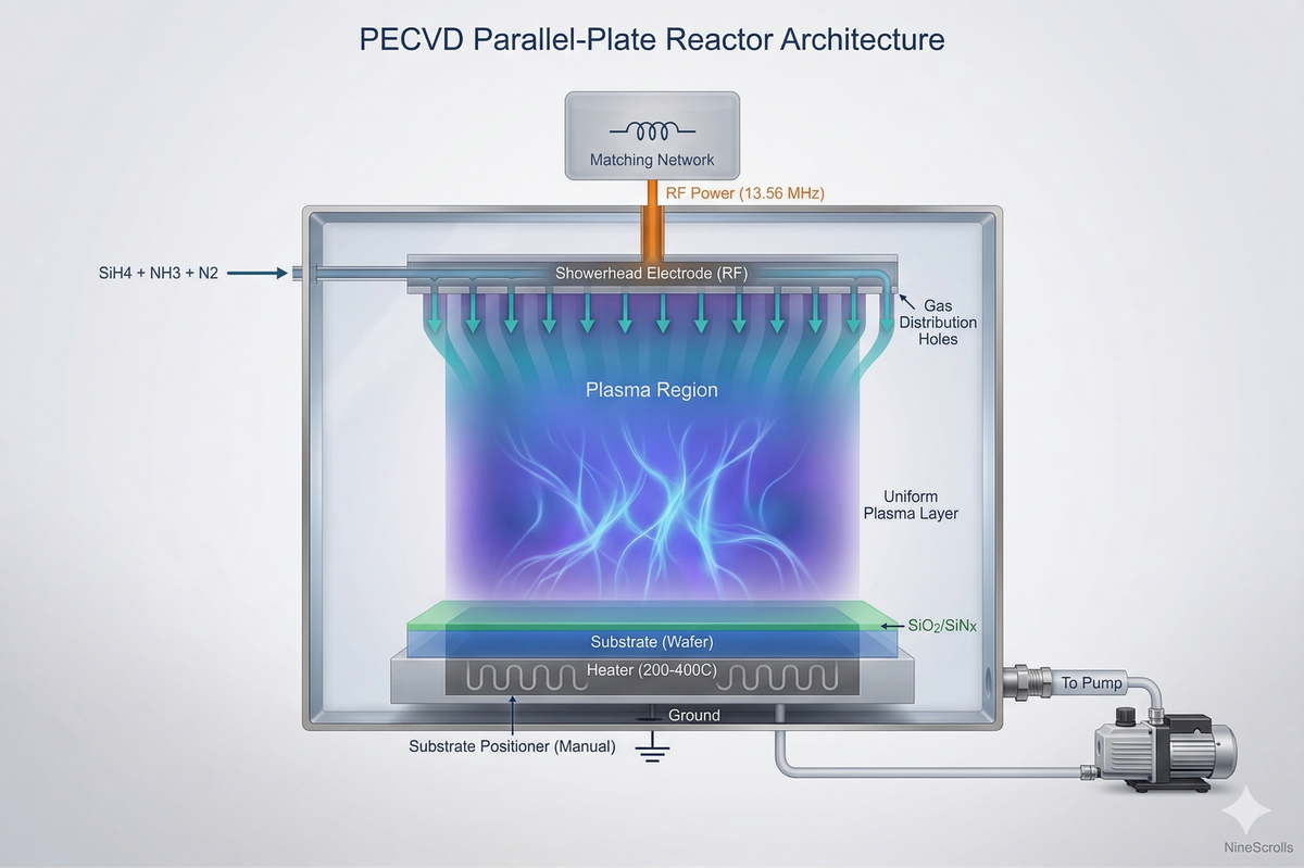
1.2 Reactor Configuration
The most common PECVD architecture is the parallel-plate (capacitively coupled plasma, CCP) reactor. The substrate sits on a heated bottom electrode (susceptor), and the RF-powered top electrode (showerhead) distributes precursor gases uniformly across the wafer. Key design parameters include:
- Electrode gap: Typically 15–40 mm. A variable gap allows optimization of plasma density and ion energy for different film chemistries. Smaller gaps increase plasma density and deposition rate but can reduce uniformity on larger wafers.
- Showerhead design: Hole pattern, diameter, and density control gas distribution. Symmetric, high-density hole patterns are essential for <5% thickness uniformity.
- Chamber liner and electrode temperature control: Heated liners (typically 50–150 °C) prevent parasitic deposition and flaking. Independent electrode temperature control suppresses particle generation.
- Substrate heating: Resistive heaters embedded in the susceptor provide 20–400 °C (higher optional) with ±2 °C uniformity across the wafer.
1.3 PECVD vs Thermal CVD: Why Plasma Matters
In thermal CVD (APCVD or LPCVD), precursor decomposition is driven entirely by substrate temperature. This imposes several constraints that PECVD overcomes:
| Parameter | Thermal CVD | PECVD |
|---|---|---|
| Substrate temperature | 600–900 °C | 20–400 °C (typically 200–350 °C) |
| Substrate compatibility | Si, quartz, ceramics only | Si, glass, metals, polymers, III–V, processed CMOS |
| Film stoichiometry control | Primarily via temperature & gas ratio | Via temperature, gas ratio, RF power, pressure, frequency |
| Stress tunability | Limited (annealing required) | Wide range: compressive to tensile via dual-frequency RF |
| Hydrogen content | Very low (high-T drives off H) | Moderate (5–25 at.% depending on conditions) |
| Throughput | High (batch furnace, 100+ wafers) | Moderate (single-wafer or small-batch) |
The hydrogen incorporated in PECVD films (primarily as Si–H and N–H bonds) is the principal trade-off: it reduces film density relative to thermal oxide but enables unique properties such as excellent surface passivation in α-Si:H solar cells and tunable refractive index in SiOₓNₙ optical films.
2) Single-Frequency vs Dual-Frequency PECVD
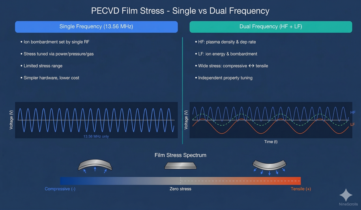
2.1 Single-Frequency Operation (13.56 MHz)
In a conventional single-frequency PECVD system, a single RF generator at 13.56 MHz (the ISM-band standard) powers the top electrode or the bottom electrode. This frequency is high enough that ions cannot follow the oscillating field cycle-by-cycle; their energy is determined by the time-averaged DC self-bias. Electrons, however, respond instantaneously, sustaining the plasma.
At 13.56 MHz, the ion bombardment energy is relatively low and the flux is moderate. Films deposited under these conditions tend to be:
- Tensile or mildly compressive, depending on deposition temperature and gas chemistry
- Moderate density (lower ion bombardment means less densification)
- Good uniformity when paired with proper showerhead design
Single-frequency PECVD is adequate for many applications — passivation layers, etch-stop films, and optical coatings where stress requirements are not stringent.
2.2 Dual-Frequency Operation (13.56 MHz + 400 kHz)
Dual-frequency PECVD adds a low-frequency (LF) generator, typically at 400 kHz, to the high-frequency (HF) excitation. The two frequencies serve distinct physical roles:
- High frequency (13.56 MHz): Primarily responsible for plasma generation and radical production. Controls deposition rate and film chemistry.
- Low frequency (400 kHz): At this frequency, ions can partially follow the RF oscillation, gaining significantly higher sheath energy. The LF component controls ion bombardment energy and therefore film densification, stress, and hydrogen content.
By adjusting the HF-to-LF power ratio, engineers achieve independent control over two normally coupled parameters:
| LF Power Fraction | Ion Energy | Film Stress | Density | H Content |
|---|---|---|---|---|
| 0% (HF only) | Low (~20–50 eV) | Tensile (+100 to +300 MPa) | Lower | Higher |
| 20–40% | Moderate (~50–150 eV) | Near-zero (±50 MPa) | Moderate | Moderate |
| 50–80% | High (~150–300 eV) | Compressive (−100 to −500 MPa) | Higher | Lower |
This stress-tuning capability is essential for:
- Multi-layer stacks: Balancing compressive and tensile layers to achieve a net-zero stress stack, preventing wafer bow
- MEMS membranes: Precise tensile stress in SiNₓ membranes for resonators and pressure sensors
- Strained-channel transistors: Depositing high-stress SiNₓ liners to induce channel strain in NMOS/PMOS
- Thick film applications: Films >2 µm without cracking or delamination
2.3 Practical Stress Engineering
A systematic approach to stress tuning in dual-frequency PECVD:
- Start with HF-only: Establish baseline deposition rate and film composition at 13.56 MHz only. Measure stress by wafer curvature (Stoney’s equation).
- Add LF incrementally: Introduce 400 kHz power in 10–20% steps while holding total power constant. Measure stress at each step to map the stress-vs-LF curve.
- Fine-tune with pressure: Higher pressure reduces mean free path and softens ion bombardment, shifting stress toward tensile. Lower pressure intensifies bombardment.
- Verify with thickness series: Deposit 100 nm, 500 nm, 1 µm, and 2 µm films at the target recipe. Stress should remain constant with thickness (if it drifts, thermal effects or gas depletion may need correction).
3) Key Film Types & Process Recipes
The following table provides representative starter recipes for the six most common PECVD film types. These are baseline windows — actual optimum conditions depend on equipment geometry, wafer size, and application requirements.
| Film | Precursors | Temp (°C) | Pressure (mTorr) | RF Power | Dep. Rate (Å/min) | Key Properties |
|---|---|---|---|---|---|---|
| SiO₂ | SiH₄ + N₂O (or TEOS + O₂) | 200–350 | 500–1500 | 100–500 W HF | 500–2000 | n = 1.45–1.47; k ≈ 0 at 633 nm; low stress with DF tuning |
| SiNₓ | SiH₄ + NH₃ (+ N₂) | 200–400 | 500–2000 | 100–800 W HF/LF | 300–1500 | n = 1.8–2.1; tunable stress −1000 to +500 MPa; excellent barrier |
| α-Si:H | SiH₄ (+ H₂) | 150–300 | 200–1000 | 50–300 W HF | 50–500 | Bandgap 1.7–1.9 eV; H content 8–15 at.%; low defect density for PV |
| SiC | SiH₄ + CH₄ (+ H₂) | 200–350 | 500–1500 | 200–600 W HF | 200–800 | k < 0.5 at 633 nm; etch stop / Cu barrier; hardness >15 GPa |
| SiON | SiH₄ + N₂O + NH₃ | 200–350 | 500–1500 | 100–500 W HF | 300–1000 | n = 1.47–1.9 (tunable); ARC for lithography; graded-index stacks |
| DLC | CH₄ (or C₂H₂) + H₂ / Ar | 20–200 | 50–500 | 200–1000 W LF-biased | 50–300 | Hardness 10–40 GPa; low friction; biocompatible; sp³ >40% |
Notes on gas chemistry selection:
- SiH₄ + N₂O vs TEOS + O₂ for SiO₂: SiH₄-based processes offer higher deposition rates and simpler gas handling. TEOS-based processes produce better step coverage (conformal coating) due to surface-mobility-driven growth, but require a liquid delivery system (bubbler or DLI) and higher substrate temperatures (≥350 °C).
- NH₃ vs N₂ for SiNₓ: NH₃ provides higher nitrogen incorporation rates and lower deposition temperatures but increases hydrogen content (N–H bonds). N₂-based processes produce lower-H films but require higher RF power for N₂ dissociation.
- H₂ dilution for α-Si:H: Increasing H₂/SiH₄ ratio promotes the transition from amorphous to microcrystalline silicon (µc-Si:H), reduces defect density, and improves carrier mobility — critical for high-efficiency solar cells and TFT active layers.
4) PECVD vs Other Deposition Methods
Choosing the right deposition technique requires understanding the trade-offs across temperature budget, conformality, throughput, and film quality. The following comparison positions PECVD relative to the five most common alternatives. For an in-depth treatment of HDP-CVD specifically, see our HDP-CVD In-Depth Guide.
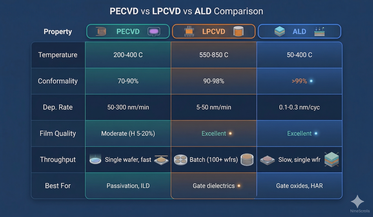
| Method | Temp (°C) | Pressure | Conformality | Gap Fill | Throughput | Film Quality | Best Use Cases |
|---|---|---|---|---|---|---|---|
| PECVD | 20–400 | 0.1–5 Torr | Moderate (50–80% step coverage) | Fair (AR <2:1) | Moderate–High | Good (contains 5–25% H) | Passivation, ILD, ARC, encapsulation, PV |
| Thermal CVD (APCVD) | 350–500 | ~760 Torr | Poor (mass-transport limited) | Poor | Very High | Moderate | PSG/BPSG reflow, flat blanket films |
| LPCVD | 550–850 | 0.1–1 Torr | Excellent (near 100%) | Good | Very High (batch) | Excellent (stoichiometric, dense) | Gate dielectrics, hardmasks, poly-Si |
| HDP-CVD | 200–400 | <10 mTorr | Moderate–Good | Excellent (AR >5:1) | Moderate | Very Good (dense, low H) | STI fill, IMD, TSV, HAR gap fill |
| ALD | 50–400 | 0.1–1 Torr | Perfect (100% by definition) | Excellent | Low (1–2 Å/cycle) | Excellent | High-k gate, <10 nm films, 3D NAND |
| Sputtering (PVD) | 20–300 | 1–10 mTorr | Poor (line-of-sight) | Poor | High | Good (dense, no H) | Metals, TCOs, seed layers, optical coatings |
When to choose PECVD over alternatives:
- Over LPCVD: When your substrate cannot tolerate >400 °C (e.g., back-end-of-line metallization, polymer substrates, compound semiconductors).
- Over HDP-CVD: When gap-fill of high-aspect-ratio features is not required and you need lower equipment cost, simpler maintenance, or wider material versatility (DLC, α-Si:H). For demanding gap-fill applications, see our HDP-CVD guide.
- Over ALD: When film thickness exceeds ~50 nm and cycle-by-cycle thickness control is unnecessary. PECVD is 10–100× faster for thick films.
- Over sputtering: When you need conformal coverage over topography, tunable composition (SiOₓNₙ), or in-situ multi-layer stacks without breaking vacuum.
5) Applications
5.1 Surface Passivation
PECVD SiNₓ and SiO₂ are the dominant passivation films in semiconductor manufacturing:
- Silicon solar cells: PECVD SiNₓ:H (n ≈ 2.0–2.1, ~75 nm) serves as both anti-reflection coating and surface passivation layer. The hydrogen content passivates dangling bonds at the Si surface, reducing surface recombination velocity to <10 cm/s. Dual-frequency PECVD enables precise control of the Si–N–H/Si–H bond ratio, directly impacting passivation quality.
- III–V devices: Low-temperature (<200 °C) PECVD SiO₂ and SiNₓ passivate GaAs, InP, and GaN surfaces without thermal degradation of the compound semiconductor.
- Final passivation (semiconductor): A SiO₂/SiNₓ bilayer or SiON single layer protects completed ICs from moisture, mobile ions (Na⁺, K⁺), and mechanical damage during packaging.
5.2 Interlayer Dielectrics (ILD)
PECVD SiO₂ serves as the primary interlayer dielectric in back-end-of-line (BEOL) interconnect stacks where thermal budget is constrained to <400 °C by copper metallization. Low-k variants (SiOC:H, fluorinated SiO₂) deposited by PECVD reduce RC delay in advanced interconnects. For features with aspect ratios exceeding 2:1, HDP-CVD or ALD may be required for void-free fill — but PECVD remains the workhorse for planar ILD layers between metal levels.
5.3 Anti-Reflection Coatings (ARC)
PECVD SiON and SiNₓ are widely used as bottom anti-reflection coatings (BARC) in optical lithography. The refractive index is tuned by adjusting the N₂O/NH₃ gas ratio, allowing precise index matching at the exposure wavelength (193 nm, 248 nm, 365 nm). PECVD ARC films offer advantages over spin-on BARC in terms of etch selectivity, conformality over topography, and elimination of organic outgassing during exposure.
5.4 Encapsulation & Barrier Layers
- OLED encapsulation: Alternating PECVD SiNₓ/SiO₂ multilayers provide water vapor transmission rates (WVTR) below 10⁻⁶ g/m²/day at substrate temperatures compatible with flexible polymer substrates (<100 °C).
- Medical device coatings: PECVD DLC and SiO₂ provide biocompatible, chemically inert barriers on implants and diagnostic devices.
- Cu diffusion barrier: PECVD SiC and SiCN serve as Cu diffusion barriers and etch-stop layers in dual-damascene interconnect architectures.
5.5 MEMS & Microsystems
PECVD films play multiple structural and functional roles in MEMS fabrication:
- Structural membranes: Low-stress SiNₓ (dual-frequency tuned to +50–+200 MPa tensile) for pressure sensors, microphones, and bolometers.
- Sacrificial layers: α-Si:H deposited by PECVD, later removed by XeF₂ vapor etch, to create free-standing structures.
- Electrical isolation: SiO₂ between conductive layers in capacitive and piezoelectric MEMS.
- Optical MEMS: Graded-index SiOₓNₙ stacks for Fabry–Pérot filters and tunable optical cavities.
5.6 Photovoltaics
PECVD is central to photovoltaic manufacturing beyond passivation:
- Heterojunction (HJT) solar cells: Intrinsic and doped α-Si:H layers deposited at <200 °C form the core of silicon heterojunction cells achieving >26% efficiency.
- Thin-film silicon: α-Si:H and µc-Si:H absorber layers for flexible and building-integrated PV.
- TCO-compatible processes: Low deposition temperatures preserve the conductivity and transparency of underlying TCO (ITO, ZnO:Al) layers.
6) Process Optimization
6.1 Thickness Uniformity
Achieving <5% thickness uniformity (with standard edge exclusion) requires systematic optimization of several interacting parameters:
- Electrode gap: Adjust the discharge gap to balance plasma density profile with gas residence time. Narrower gaps improve center-to-edge uniformity on smaller wafers; wider gaps are needed for 200 mm and 300 mm substrates.
- Pressure: Higher pressure increases gas-phase reactions and may cause non-uniform radical distribution. Typical sweet spot: 500–1500 mTorr for SiO₂ and SiNₓ.
- Gas flow distribution: Showerhead zone control (if available) or total flow rate adjustment. Insufficient flow starves the wafer edge; excessive flow wastes precursor and may increase particulate generation.
- Temperature uniformity: Even 5 °C variation across the susceptor can produce 2–3% thickness non-uniformity due to temperature-dependent surface reaction rates. Multi-zone heater control is recommended for wafers ≥6”.
- Electrode condition: Monitor electrode surface condition. Dielectric buildup on the powered electrode shifts the plasma and degrades uniformity. Regular in-situ plasma cleaning (NF₃ or CF₄/O₂) between deposition runs maintains consistent performance.
6.2 Film Stress Control
Beyond the dual-frequency approach described in Section 2, additional stress-tuning levers include:
- Deposition temperature: Higher substrate temperature generally shifts stress toward compressive (due to thermal mismatch on cooling) and reduces hydrogen content.
- Post-deposition anneal: Rapid thermal anneal (RTA) at 400–600 °C for 30–60 s drives out hydrogen and densifies the film, shifting stress toward compressive by 100–300 MPa. Useful when the deposition must occur at low temperature but higher film quality is needed.
- Gas ratio: For SiNₓ, increasing the SiH₄/NH₃ ratio produces Si-rich films that tend toward compressive stress (and higher refractive index). N-rich films (high NH₃) are more tensile.
- Plasma power: Higher total RF power increases ion bombardment and generally produces more compressive films, but may also increase defect density. The dual-frequency approach provides finer control than simply increasing single-frequency power.
6.3 Refractive Index Control
Refractive index is a sensitive indicator of film composition and density. For optical applications (ARC, waveguides, filters), precise index control is essential:
- SiO₂: Target n = 1.46 ± 0.01 at 633 nm. Low index indicates porosity or excess oxygen; high index suggests Si-rich composition or densification.
- SiNₓ: Tunable from n = 1.8 (N-rich) to n = 2.2 (Si-rich) by adjusting SiH₄/NH₃ ratio. Stoichiometric Si₃N₄ corresponds to n ≈ 2.0.
- SiON: Continuously tunable from n = 1.46 (SiO₂) to n = 2.0 (SiNₓ) by varying N₂O/NH₃ flow ratio. This enables graded-index structures in a single deposition chamber.
- α-Si:H: n = 3.5–4.0 at 633 nm; extinction coefficient k is strongly temperature-dependent. For waveguide applications, higher deposition temperature reduces k by improving atomic ordering.
6.4 Adhesion Improvement
Poor adhesion is the most common failure mode in multi-layer PECVD stacks. Systematic approaches include:
- Surface preparation: Immediately before deposition, run an in-situ Ar or O₂ plasma treatment (30–60 s, low power) to remove native oxide, organic contaminants, and surface moisture. This step alone resolves >70% of adhesion failures.
- Interfacial layer: Deposit a thin (<20 nm) adhesion-promoting layer. SiO₂ on metal, SiNₓ on polymer, or a-Si:H on glass all improve cross-material adhesion.
- Graded composition: For SiOₓNₙ stacks, ramping the gas ratio during the first 20–50 nm creates a compositional gradient that reduces the abrupt stress discontinuity at the interface.
- Stress matching: Ensure the film stress is compatible with the substrate. Highly compressive films on thin wafers or polymer substrates cause delamination at the edges. Reduce LF power or increase deposition temperature to shift toward neutral stress at interfaces.
6.5 Particle & Defect Control
Particle adders directly impact device yield. Key strategies for maintaining low particle counts in PECVD:
- Chamber conditioning: After wet cleaning or maintenance, run 5–10 conditioning (dummy) depositions before processing production wafers. This coats all exposed chamber surfaces with a uniform film, preventing flaking from dissimilar thermal expansion.
- In-situ cleaning frequency: Clean the chamber with NF₃ or CF₄/O₂ plasma every 1–5 µm of cumulative deposition, depending on film type. SiNₓ and α-Si:H generate more particulates than SiO₂ and require more frequent cleaning.
- Chamber liner temperature: Maintaining the liner at 50–150 °C prevents gas-phase nucleation (too cold) and thermal stress cracking of deposited films on the liner (too hot).
- Process pressure: Excessively high pressure (>3 Torr for SiH₄-based processes) promotes gas-phase polymerization and powder formation. Monitor for upstream pressure spikes that indicate particulate generation.
7) Equipment Selection Guide
Selecting a PECVD system requires matching equipment capabilities to your application requirements. The following checklist covers the critical evaluation criteria:
7.1 Wafer Size & Format
- Research & prototyping (4”–6”): Single-wafer systems with manual or semi-automatic loading. Lower cost, faster recipe iteration, minimal cleanroom footprint.
- Pilot line (6”–8”): Single-wafer with cassette-to-cassette automation. Enables process qualification on production-representative wafers.
- Production (8”–12”): Fully automated single-wafer or multi-wafer (batch) systems with load-lock, robotic transfer, and in-situ cleaning. Multi-wafer configurations improve throughput for thick films.
7.2 RF Configuration
- Single-frequency (13.56 MHz): Sufficient for basic oxide and nitride deposition where stress specification is ±300 MPa or wider. Lower system cost.
- Dual-frequency (13.56 MHz + 400 kHz): Required for stress-engineered films (MEMS membranes, strained liners, thick films >2 µm), DLC deposition, and applications requiring independent control of deposition rate and film density. Power range of 500–2000 W per generator provides flexibility from gentle low-power processes to high-rate production recipes.
7.3 Temperature Range
- Standard (200–400 °C): Covers the majority of dielectric and semiconductor film applications.
- Low-temperature (20–200 °C): Essential for polymer substrates (flexible electronics, OLED), temperature-sensitive devices (HgCdTe IR detectors), and post-metallization processing. Requires active substrate cooling and process pressure optimization to maintain film quality at reduced temperatures.
- Extended range (up to 500 °C+): Enables higher-quality films approaching LPCVD performance while retaining plasma-assisted deposition benefits.
7.4 Gas Delivery
- Number of gas lines: 4 lines minimum for basic SiO₂ and SiNₓ. 6 lines recommended for multi-material flexibility (SiH₄, NH₃, N₂O, N₂, Ar, CH₄ or NF₃).
- Mass flow controllers: Choose MFC ranges appropriate for your gas flows. Low-flow (<50 sccm) MFCs may be needed for dopant gases or precise stoichiometry control. High-flow (>1 slm) MFCs are needed for carrier and cleaning gases.
- Liquid delivery: If TEOS-based SiO₂ is required, ensure the system supports a heated liquid source (bubbler or direct liquid injection).
7.5 Process Monitoring & Control
- In-situ thickness monitoring: Laser reflectance or spectroscopic ellipsometry for real-time rate and endpoint control.
- Plasma diagnostics: Optical emission spectroscopy (OES) for plasma stability monitoring and cleaning endpoint detection.
- Residual gas analysis (RGA): Mass spectrometer for leak detection, gas purity verification, and cleaning endpoint confirmation.
- Recipe management: Software with multi-step recipe capability, ramped parameter profiles, and data logging for SPC and process traceability.
7.6 NineScrolls PECVD Systems
NineScrolls PECVD systems are designed to address the full range of requirements outlined above:
- Wafer sizes: 4”, 6”, 8”, 12”, and multi-wafer configurations
- RF system: 13.56 MHz and/or 400 kHz dual-frequency, 500–2000 W per generator
- Temperature: 20 °C to 400 °C standard (higher optional)
- Gas lines: Up to 6 independently controlled MFC channels
- Uniformity: <5% thickness non-uniformity (standard edge exclusion)
- Materials: α-Si:H, SiO₂, SiNₓ, SiC, SiON, DLC
- Key differentiators: Variable plasma discharge gap for process flexibility, independent chamber liner and electrode temperature control for reduced particle generation, and dual-frequency RF for full stress tunability from compressive to tensile
For detailed specifications, configurations, and pricing, visit the PECVD product page or contact our applications engineering team.
Frequently Asked Questions
What is the difference between PECVD and LPCVD?
The primary difference is the energy source for precursor decomposition. LPCVD relies entirely on thermal energy (550–850 °C), producing dense, stoichiometric, hydrogen-free films with excellent step coverage in a batch furnace. PECVD uses plasma energy to enable deposition at 20–400 °C, making it compatible with temperature-sensitive substrates, but films contain 5–25 at.% hydrogen and have lower density. LPCVD is preferred for front-end-of-line films (gate dielectrics, hardmasks) where thermal budget is available; PECVD is the standard for back-end-of-line and any process with temperature constraints below 500 °C.
How do I reduce hydrogen content in PECVD films?
Hydrogen incorporation can be reduced through several approaches: (1) Increase substrate temperature — every 50 °C increase typically reduces H content by 2–4 at.% by promoting H₂ desorption. (2) Increase LF (400 kHz) power fraction — higher ion bombardment energy sputters weakly-bonded hydrogen from the growing film. (3) Use N₂ instead of NH₃ as the nitrogen source for SiNₓ — eliminates N–H bonds at the cost of lower deposition rate. (4) Post-deposition anneal at 400–600 °C drives out bonded hydrogen. (5) Increase H₂ dilution ratio for α-Si:H — counterintuitively, excess H₂ etches weak Si–H bonds during growth, yielding a more ordered network with lower total H content.
Can PECVD achieve void-free gap fill in high-aspect-ratio trenches?
Standard PECVD provides reliable void-free fill for aspect ratios up to approximately 1.5–2:1. Beyond this, the non-conformal deposition profile (faster growth at feature tops than bottoms) causes the opening to pinch off before the trench is completely filled, creating a keyhole void. For aspect ratios exceeding 2:1, consider: (1) PECVD with dep-etch cycling (alternating deposition and argon sputter-back steps), which extends gap-fill capability to ~3:1; (2) HDP-CVD, which uses simultaneous deposition and sputtering for void-free fill at aspect ratios >5:1 (see our HDP-CVD guide); or (3) ALD for extreme aspect ratios (>50:1) where perfect conformality is required.
What is the typical chamber cleaning frequency for PECVD?
In-situ plasma cleaning (NF₃ or CF₄/O₂) should be performed every 1–5 µm of cumulative deposited thickness on the chamber walls. For production environments, a common rule of thumb is to clean after every 3–5 wafer runs for SiNₓ and α-Si:H processes (which generate more particulates) and every 5–10 runs for SiO₂. The optimal frequency depends on your particle specification — tighter requirements (<50 adders >0.1 µm) demand more frequent cleaning. Full wet cleaning (chamber open, manual wipe-down and part replacement) is typically done every 50–100 RF-hours or when particle counts exceed specification despite in-situ cleaning.
Why is dual-frequency PECVD important for MEMS fabrication?
MEMS devices often require precise, reproducible film stress. Pressure sensor membranes need mild tensile stress (+50 to +200 MPa) to remain taut without buckling; resonators need specific stress for target resonant frequency; and multi-layer stacks must be stress-balanced to prevent wafer bow during release etching. Dual-frequency PECVD provides the only practical way to independently set deposition rate (via HF power) and film stress (via LF power fraction) during a single deposition step. Single-frequency systems force a trade-off: changing power to adjust stress simultaneously changes deposition rate, composition, and uniformity. With dual-frequency control, MEMS engineers can target a stress specification within ±20 MPa while maintaining all other film properties.
What substrate materials are compatible with PECVD?
PECVD’s low-temperature capability makes it compatible with virtually any substrate that can survive moderate vacuum: silicon wafers, glass, quartz, sapphire, GaAs, InP, GaN, SiC, stainless steel, aluminum, copper, titanium, Kapton polyimide, PET, PEN, PDMS, and even paper (with appropriate temperature settings). The key constraint is the substrate’s maximum temperature tolerance — PECVD can operate from room temperature to 400 °C (and higher with specialized configurations), so the process temperature is simply matched to the substrate’s limit. Secondary considerations include substrate outgassing (polymers may require pre-bake), CTE mismatch (which affects film adhesion and stress), and electrical conductivity (insulating substrates may charge in the plasma, requiring grounding strategies).
How does PECVD film quality compare to thermal oxide?
Thermal oxide (grown at 900–1100 °C) remains the gold standard for SiO₂ quality: density of 2.2 g/cm³, breakdown field >10 MV/cm, negligible hydrogen content, and near-perfect Si/SiO₂ interface quality. PECVD SiO₂ deposited at 300–400 °C typically achieves density of 2.1–2.2 g/cm³, breakdown field of 5–8 MV/cm, 5–15 at.% hydrogen, and an interface quality that depends on surface preparation and deposition conditions. For gate dielectric applications requiring the highest reliability, thermal oxide or ALD remains necessary. However, for passivation, ILD, optical coatings, and encapsulation, PECVD oxide performance is more than adequate and the low-temperature advantage is decisive.
What safety precautions are required for PECVD operation?
PECVD processes involve several hazards requiring appropriate controls: (1) Toxic and pyrophoric gases: SiH₄ is pyrophoric (spontaneously ignites in air); NH₃ and NF₃ are toxic. Gas cabinets with automatic shutoff valves, toxic gas monitoring, and fire suppression are mandatory. (2) RF radiation: Ensure proper shielding of all RF connections. Interlock the chamber lid so RF cannot energize with the chamber open. (3) High voltage: RF matching networks contain high-voltage capacitors. Follow lockout/tagout procedures during maintenance. (4) Vacuum hazards: Chamber implosion risk with glass viewports; use laminated or polycarbonate-shielded viewports. (5) Chemical exposure during maintenance: Deposited films and chamber residues may contain silane decomposition products. Use appropriate PPE (gloves, respirator) during wet cleaning. Consult the safety data sheets for all process gases and follow your facility’s environmental health and safety protocols.
NineScrolls PECVD Systems
Engineered for precision thin-film deposition with dual-frequency RF stress control, variable discharge gap, and chamber thermal management — from research-scale 4” to production 12” and multi-wafer configurations.