Magnetron Sputtering – Principles, Process Parameters, and Equipment Guide
By NineScrolls Engineering · 2026-03-27 · 18 min read · Materials Science
Target Readers: Thin-film process engineers, materials scientists, equipment engineers, PIs/lab managers, and technical decision-makers evaluating PVD deposition solutions. Newcomers to sputtering will find the fundamentals and parameter tables helpful; experienced engineers can skip to the film optimization and equipment selection sections.
TL;DR Summary
Magnetron sputtering is a plasma-based physical vapor deposition (PVD) technique that uses magnetically confined plasma to eject atoms from a solid target onto a substrate, producing high-quality thin films of metals, oxides, nitrides, and compound semiconductors. By tuning parameters such as power mode (DC vs RF), working pressure, gas composition, substrate temperature, and target–substrate distance, engineers achieve precise control over film thickness, uniformity, stress, adhesion, and microstructure. This guide covers the underlying physics, compares DC and RF sputtering modes, explains reactive sputtering for compound films, provides process parameter windows, and offers a complete equipment selection framework—everything needed to design, optimize, and scale a magnetron sputtering process.
1) What is Magnetron Sputtering?
1.1 Basic Principles
Sputtering is a momentum-transfer process: energetic ions (typically Ar⁺) from a plasma are accelerated toward a solid target (cathode), ejecting surface atoms through collision cascades. These sputtered atoms traverse the vacuum chamber and condense on the substrate to form a thin film. The technique was first described by Grove in 1852, but practical thin-film sputtering required the development of vacuum technology and, critically, the magnetron configuration in the 1970s.
The key physics governing sputter yield (atoms ejected per incident ion) include:
- Ion energy: Higher cathode voltage increases sputter yield, but above a material-dependent threshold (~1–2 keV for most metals), yield gains diminish while substrate damage increases
- Ion mass: Heavier sputtering gases (Kr, Xe) increase momentum transfer but are rarely cost-effective; Ar is the universal standard
- Target material: Sputter yields vary from ~0.1 (C, Si) to ~3.0 (Ag, Au) at 500 eV Ar⁺. Refractory metals (W, Mo, Ta) have yields of 0.4–0.6
- Angle of incidence: Maximum sputter yield typically occurs at 60–80° from normal, which influences the erosion profile on planar targets
1.2 The Magnetron Advantage
In conventional diode sputtering, electrons travel in straight paths between cathode and anode, resulting in low ionization efficiency and requiring high pressures (>100 mTorr) that cause excessive gas-phase scattering. The magnetron configuration solves this by placing permanent magnets behind the target to create a closed magnetic field (typically 200–500 Gauss at the target surface). This field traps secondary electrons in helical paths near the target surface, dramatically increasing the electron path length and ionization probability.
The consequences are transformative:
- 10–100× higher plasma density near the target surface compared to diode sputtering
- Lower operating pressures (1–10 mTorr vs 50–100 mTorr), reducing gas-phase scattering and improving film density
- Higher deposition rates at lower voltages, reducing substrate heating from energetic neutrals
- Lower substrate damage from reduced electron bombardment, since electrons are confined near the cathode
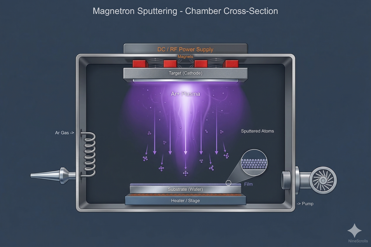
1.3 Plasma Generation and Target Erosion
When a negative voltage (−300 to −700 V for DC; self-bias for RF) is applied to the target, the process proceeds through several stages:
- Gas breakdown: Free electrons are accelerated by the electric field and ionize argon atoms (ionization energy = 15.76 eV), creating an Ar⁺/e⁻ plasma
- Sheath formation: A dark space (Crookes dark space) forms at the cathode where the full target voltage drops across a few Debye lengths (~0.1–1 mm)
- Ion bombardment: Ar⁺ ions are accelerated across the cathode sheath and strike the target, initiating collision cascades in the top 1–3 nm of the target surface
- Atom ejection: Target atoms with sufficient energy to overcome the surface binding energy (typically 3–8 eV) are ejected with a cosine angular distribution and kinetic energies of 1–30 eV
- Secondary electron emission: Each ion impact also releases 0.05–0.2 secondary electrons that are trapped by the magnetic field, sustaining the plasma
The sputtered atoms travel through the gas phase, undergoing thermalization (energy loss through gas-phase collisions). At typical working pressures (3–5 mTorr), the mean free path is 1–3 cm, meaning atoms arriving at the substrate (5–15 cm away) have undergone multiple collisions and arrive with energies of 0.1–1 eV. This is significantly more energetic than thermally evaporated atoms (~0.1 eV), contributing to denser, better-adhered films.
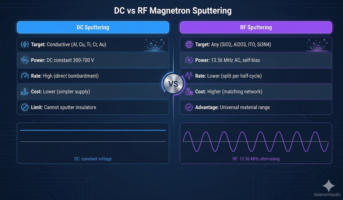
2) DC vs RF Sputtering
2.1 DC Magnetron Sputtering
DC (direct current) sputtering applies a constant negative voltage to the target. It is the simplest, most efficient, and highest-rate sputtering mode, but it requires the target to be electrically conductive. If the target surface becomes insulating (e.g., from oxide formation during reactive sputtering), positive charge accumulates on the surface, reducing the effective voltage and eventually extinguishing the plasma—a phenomenon called target poisoning or disappearing anode.
When to use DC sputtering:
- Depositing pure metals: Al, Cu, Ti, Cr, Pt, Pd, W, Ru, Mo, Ta, Ni, Co
- Metallic alloys and metal silicides
- When maximum deposition rate is needed (DC rates are typically 2–5× higher than RF for the same power)
- Reactive sputtering of nitrides from metallic targets (with appropriate feedback control)
2.2 RF Magnetron Sputtering
RF (radio frequency, 13.56 MHz) sputtering uses an alternating voltage that allows charge neutralization on insulating target surfaces during each positive half-cycle. The key physics: because electrons are much more mobile than ions, the target self-biases to a negative DC potential even though the applied voltage is symmetric. This self-bias drives ion bombardment of the target while preventing charge buildup.
When to use RF sputtering:
- Insulating targets: SiO₂, Al₂O₃, BaTiO₃, PZT, HfO₂, ZnO
- Magnetic materials where target permeability reduces magnetron effectiveness (RF helps sustain plasma)
- Compound semiconductor targets: GaAs, InP, CdTe, CIGS
- When stoichiometric transfer from a compound target is required
- RF-biased substrate cleaning (in-situ pre-deposition sputter etch)
2.3 DC vs RF Comparison
| Parameter | DC Sputtering | RF Sputtering |
|---|---|---|
| Target material | Conductors only | Conductors and insulators |
| Deposition rate | High (1–20 Å/s typical) | Lower (0.5–5 Å/s typical) |
| Power efficiency | High (~80% to plasma) | Lower (~50–60% due to matching losses) |
| Power supply cost | Lower | Higher (RF generator + matchbox) |
| Arcing risk | Higher with reactive gases | Lower (self-neutralizing) |
| Stoichiometry control | Reactive gas flow required | Direct from compound target |
| Substrate bias | Separate bias supply needed | Inherent or separate RF bias |
3) Reactive Sputtering
3.1 Principles
Reactive sputtering introduces a reactive gas (O₂, N₂, or a mixture) alongside the inert sputtering gas (Ar) to form compound films—oxides, nitrides, oxynitrides, and carbides—from metallic targets. The reactive gas participates in film formation through three pathways:
- At the substrate: Sputtered metal atoms react with adsorbed reactive gas molecules on the growing film surface (dominant pathway)
- In the gas phase: Metal atoms react with reactive gas molecules during transit (minor contribution at low pressures)
- At the target: Reactive gas reacts with the target surface, forming a compound layer (target poisoning—generally undesirable)
3.2 The Hysteresis Problem
Reactive sputtering exhibits a well-known hysteresis effect as reactive gas flow is varied. In the metallic mode (low reactive gas flow), the target surface remains metallic, deposition rates are high, but films may be sub-stoichiometric. In the poisoned mode (high reactive gas flow), the target surface is fully reacted, sputter yield drops dramatically (sometimes 10×), and the excess reactive gas is no longer consumed—causing a sudden jump in chamber partial pressure.
The transition between these modes is abrupt and exhibits hysteresis: the flow at which poisoning occurs (increasing flow) is higher than the flow at which the target recovers (decreasing flow). The ideal operating point is often in the unstable transition zone between metallic and poisoned modes, where stoichiometric films can be deposited at reasonable rates.
3.3 Controlling Reactive Sputtering
Stable operation in the transition zone requires feedback control. Common approaches include:
- Optical emission spectroscopy (OES): Monitor a characteristic emission line of the sputtered metal; as the target poisons, metal emission drops. PID feedback adjusts reactive gas flow to maintain a setpoint intensity
- Partial pressure control: A fast-response capacitance manometer or RGA monitors the reactive gas partial pressure; a feedback loop adjusts the mass flow controller
- Cathode voltage monitoring: Target voltage changes with surface composition (e.g., voltage increases for oxide-covered targets). Simple but less sensitive than OES
- Pulsed DC sputtering: Mid-frequency pulsing (20–350 kHz) periodically neutralizes charge on partially poisoned target surfaces, preventing arcing and enabling operation closer to the transition zone without full feedback control
3.4 Common Reactive Sputtering Processes
| Film | Target | Reactive Gas | Typical Applications |
|---|---|---|---|
| TiN | Ti | N₂ (5–30% of total flow) | Hard coatings, diffusion barriers, decorative gold color |
| AlN | Al | N₂ (30–70% of total flow) | Piezoelectric films, GaN buffer layers, MEMS resonators |
| SiO₂ | Si | O₂ (10–50% of total flow) | Optical coatings, gate dielectrics, passivation |
| Al₂O₃ | Al | O₂ (20–40% of total flow) | Dielectric layers, protective coatings, tunnel barriers |
| TiO₂ | Ti | O₂ (10–40% of total flow) | Photocatalysis, high-k dielectrics, optical filters |
| SiNₓ | Si | N₂ (40–80% of total flow) | Passivation, etch stop, anti-reflection coatings |
| WN | W | N₂ (10–30% of total flow) | Cu diffusion barriers, low-resistivity contacts |
4) Key Process Parameters
Magnetron sputtering involves a multi-dimensional parameter space. Understanding the effect of each parameter—and their interactions—is essential for process development and optimization.
4.1 Working Pressure
Working pressure (typically 1–15 mTorr for magnetron sputtering) directly affects mean free path, deposition rate, film density, and stress:
- Low pressure (1–3 mTorr): Long mean free path, energetic adatom arrival, dense columnar or zone T microstructure, compressive stress. Requires good magnetron confinement to sustain plasma
- Medium pressure (3–8 mTorr): Balanced regime for most processes. Good uniformity across larger substrates
- High pressure (8–15 mTorr): Short mean free path, thermalized adatoms, porous columnar microstructure (Zone 1 in Thornton’s structure zone model), tensile stress. Higher gas-phase scattering improves step coverage but reduces rate
4.2 Sputtering Power
Power applied to the target (DC watts or RF forward watts) controls the ion flux to the target surface:
- Deposition rate: Approximately linear with power for a given target material and pressure. Typical DC rates: Al ~15 Å/s/kW, Ti ~5 Å/s/kW, Pt ~8 Å/s/kW
- Film properties: Higher power increases adatom energy (higher sputter yield atoms), improving density and reducing resistivity, but may increase compressive stress
- Target thermal management: Target cooling must handle the heat load (70–90% of applied power becomes heat). Water-cooled magnetrons are essential above 200 W
- Power density: Expressed as W/cm² of target area. Typical range: 5–30 W/cm². Exceeding the target material’s thermal limit causes cracking (especially ceramics) or melting
4.3 Gas Flow and Composition
Process gas management involves both the sputtering gas (Ar) and any reactive gases:
- Ar flow: Set to achieve the desired working pressure at the given pumping speed. Typical: 10–50 sccm depending on chamber volume and pump throughput
- Reactive gas ratio: Critical for stoichiometry in reactive sputtering (see Section 3)
- Gas purity: Use 99.999% (5N) or better for critical applications. Even 10 ppm O₂ in Ar can degrade metallic film resistivity by 10–30%
- Gas distribution: Uniform gas injection (shower ring or distributed inlets) improves film thickness uniformity
4.4 Substrate Temperature
Substrate temperature during deposition profoundly affects film microstructure, following the Thornton structure zone model (characterized by T/Tₘ, the ratio of substrate temperature to target material melting point in Kelvin):
- Zone 1 (T/Tₘ < 0.2): Columnar grains separated by voids. Low adatom mobility. Porous, high-resistivity films
- Zone T (0.2 < T/Tₘ < 0.4): Fibrous grains without voiding. Dense, smooth films. Optimal for many applications
- Zone 2 (0.4 < T/Tₘ < 0.6): Columnar grains with dense grain boundaries. Bulk-like properties emerge
- Zone 3 (T/Tₘ > 0.6): Equiaxed recrystallized grains. Lowest resistivity but rougher surfaces
NineScrolls sputter systems support substrate temperatures from water-cooled (near ambient) up to 1200°C, covering the full range of thin-film microstructure engineering—from room-temperature amorphous barrier layers to high-temperature epitaxial growth of crystalline films like AlN and PZT.
4.5 Target–Substrate Distance
The throw distance affects deposition rate, uniformity, and film properties:
- Short throw (3–5 cm): High rate, energetic adatoms, but poor uniformity over large areas and higher substrate heating
- Long throw (10–20 cm): Better uniformity and step coverage, lower rate, more thermalized adatoms
- Optimal distance: Typically 1.5–3× the target diameter for <1% uniformity across the substrate. For multi-target systems, confocal geometry (angled targets) provides excellent uniformity through overlapping deposition zones
4.6 Substrate Bias
Applying an RF bias to the substrate (typically −25 to −150 V) provides independent control over ion bombardment of the growing film:
- Densification: Ion bombardment increases adatom mobility, collapsing voids and improving density at lower substrate temperatures
- Stress control: Moderate bias (~−50 to −100 V) drives films from tensile toward compressive stress. Over-biasing creates excessive compressive stress and can cause delamination
- Step coverage: Bias-driven resputtering from horizontal surfaces redistributes material into sidewalls, improving conformality
- In-situ cleaning: High-bias Ar⁺ bombardment before deposition removes native oxides and surface contaminants, improving adhesion. NineScrolls sputter systems feature dedicated RF-biased substrate cleaning capability for this purpose
4.7 Process Parameter Summary Table
| Parameter | Typical Range | Primary Effect | Key Trade-off |
|---|---|---|---|
| Base pressure | <5×10⁻⁷ Torr | Film purity | Pump-down time vs contamination |
| Working pressure | 1–15 mTorr | Mean free path, film density | Rate/density vs step coverage |
| DC power | 100–2000 W | Deposition rate, adatom energy | Rate vs target heating/stress |
| RF power | 300–1000 W | Deposition rate (insulators) | Power efficiency vs material range |
| Substrate temperature | RT–1200°C | Microstructure (SZM zone) | Crystallinity vs thermal budget |
| Substrate bias | −25 to −150 V | Film density, stress | Densification vs resputtering damage |
| Ar flow | 10–50 sccm | Working pressure | Pressure stability vs gas cost |
| Target–substrate distance | 5–20 cm | Uniformity, rate | Uniformity vs deposition rate |
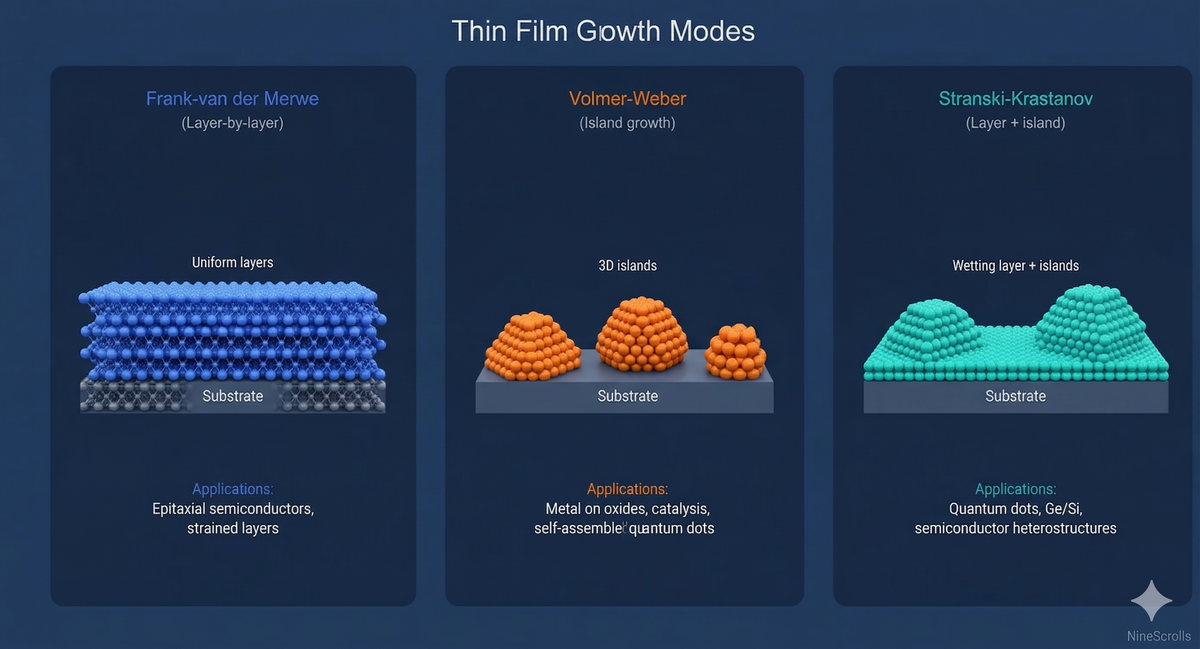
5) Common Materials and Applications
Magnetron sputtering’s versatility is unmatched among PVD techniques. The following table summarizes materials commonly deposited and their primary applications:
| Material Category | Examples | Sputtering Mode | Key Applications |
|---|---|---|---|
| Noble metals | Pt, Pd, Au, Ag, Ru, Ir | DC | Electrodes (MEMS, ferroelectric), catalysts, contacts, biosensors |
| Refractory metals | W, Mo, Ta, Nb, Ti | DC | Barrier/adhesion layers, hard masks, interconnects, superconducting qubits |
| Transition metals | Cu, Al, Cr, Ni, Co | DC | Metallization, seed layers, magnetic recording |
| Nitrides | TiN, AlN, SiNₓ, TaN, WN | Reactive DC/RF | Diffusion barriers, hard coatings, piezoelectrics, etch stops |
| Oxides | SiO₂, Al₂O₃, TiO₂, HfO₂, ITO, ZnO | Reactive DC or RF | Dielectrics, optical coatings, TCOs, high-k gates |
| Magnetic materials | CoFe, NiFe (permalloy), FePt, CoCrPt | DC/RF | TMR junctions, spintronic devices, magnetic recording media |
| Compound semiconductors | GaAs, CdTe, CIGS, ZnSe | RF | Solar cells, photodetectors, LED buffers |
| Ferroelectrics | PZT, BaTiO₃, BST | RF | MEMS actuators, FeRAM, pyroelectric sensors |
6) Sputtering vs Other PVD Techniques
Choosing the right deposition method requires understanding each technique’s strengths and limitations. The following table compares magnetron sputtering with electron-beam evaporation, thermal evaporation, pulsed laser deposition (PLD), and atomic layer deposition (ALD):
| Feature | Magnetron Sputtering | E-beam Evaporation | Thermal Evaporation | PLD | ALD |
|---|---|---|---|---|---|
| Mechanism | Ion bombardment of target | Electron beam heating | Resistive/inductive heating | Laser ablation of target | Sequential chemical reactions |
| Adatom energy | 1–30 eV | 0.1–0.3 eV | 0.1 eV | 10–100 eV | Thermal (~0.03 eV) |
| Film density | High (>95% bulk) | Moderate (85–95%) | Low–moderate (80–90%) | Very high (~100%) | Very high (~100%) |
| Deposition rate | 1–20 Å/s | 1–50 Å/s | 1–30 Å/s | 0.01–1 Å/s | 0.1–2 Å/cycle |
| Uniformity | <1% achievable | 2–5% (point source) | 3–10% | 5–15% (small plume) | <1% (self-limiting) |
| Step coverage | Moderate (10–50%) | Poor (line-of-sight) | Poor (line-of-sight) | Poor (directional plume) | Excellent (>95%) |
| Material range | Very broad (metals, oxides, nitrides) | Broad (metals, some oxides) | Limited (low-melting metals) | Excellent (complex oxides) | Limited by precursor chemistry |
| Stoichiometry control | Good (reactive or compound targets) | Poor (preferential evaporation) | Poor | Excellent (congruent transfer) | Excellent (self-limiting) |
| Scalability | Excellent (up to 12”+ wafers) | Good (planetary rotation) | Moderate | Poor (small area) | Excellent (batch processing) |
| Substrate damage | Low–moderate (UV, energetic neutrals) | Low (X-rays possible) | Very low | Moderate–high (energetic species) | Very low |
| Best for | Multi-material stacks, production coatings | High-rate metals, optical coatings | Al, Au, Ag, organic materials | Complex oxide R&D | Ultrathin conformal films |
7) Film Quality Optimization
7.1 Film Stress
Intrinsic stress in sputtered films arises from atomic-scale defects (interstitials, grain boundaries, voids) and is highly sensitive to process conditions. Understanding the stress mechanisms enables systematic optimization:
- Tensile stress originates from grain boundary voids and attractive forces across under-dense boundaries. Promoted by high pressure, low power, low substrate temperature, and large throw distance
- Compressive stress results from atomic peening—energetic species (reflected neutrals, sputtered atoms) implanting into interstitial sites. Promoted by low pressure, high power, substrate bias, and short throw distance
- Zero-stress crossing: For most materials, there exists a pressure (typically 5–10 mTorr) at which stress transitions from compressive to tensile. This crossover pressure depends on target material, power, and geometry
Practical stress control strategy:
- Start at moderate pressure (5 mTorr) and characterize stress by wafer curvature (Stoney’s equation)
- Adjust pressure first (coarse control): lower pressure → more compressive; higher pressure → more tensile
- Apply substrate bias for fine tuning: increasing bias drives films compressive
- Consider interrupted deposition (alternating deposition and stress-relief annealing) for very thick films
7.2 Adhesion
Poor adhesion is the most common sputtered-film failure mode. Root causes and solutions:
- Surface contamination: Native oxides, hydrocarbons, and adsorbed water reduce bonding. Solution: in-situ RF substrate cleaning (Ar⁺ sputter etch) immediately before deposition. NineScrolls systems include dedicated RF bias for this purpose
- Thermal mismatch: Large CTE differences between film and substrate create interfacial stress during cooling. Solution: use adhesion/buffer layers (Ti, Cr, or Ta at 5–20 nm thickness)
- Intrinsic stress: Highly stressed films can delaminate, especially thick films. Solution: optimize stress as described in Section 7.1 and limit individual layer thickness
- Chemical incompatibility: Some film/substrate combinations have poor bonding chemistry. Solution: use reactive interlayers (e.g., Ti for Pt on SiO₂, where Ti forms TiO₂ bonds to the substrate and TiPt intermetallic bonds to the film)
7.3 Uniformity
Film thickness uniformity is governed by the geometric relationship between the target erosion profile and the substrate position. For a circular magnetron target over a circular substrate:
- <1% uniformity is achievable when the substrate diameter is ≤1/3 of the target diameter and the throw distance is optimized (typically 1.5–2.5× target diameter)
- Substrate rotation during deposition averages out any azimuthal non-uniformity from gas flow patterns or target erosion asymmetry
- Multi-target confocal geometry (where 2–6 targets are tilted toward a central substrate position) provides excellent uniformity for co-deposition and multilayer stacks
- Deposition shields (shadow masks or chimney-style collimators) can improve uniformity at the expense of deposition rate
7.4 Step Coverage and Conformality
Magnetron sputtering is fundamentally a line-of-sight process, with step coverage determined by the angular distribution of arriving atoms:
- Standard sputtering: 10–30% step coverage on features with aspect ratios of 1:1 to 3:1
- Ionized PVD (high-power impulse magnetron sputtering, HiPIMS): Ionized flux can be directed by substrate bias, achieving 50–80% step coverage in trenches
- RF substrate bias: Concurrent resputtering redistributes material from field areas to sidewalls, improving coverage to 30–50% for standard magnetron sputtering
- Collimated sputtering: Honeycomb collimator between target and substrate filters oblique atoms, improving bottom coverage at the expense of rate
For applications requiring >90% step coverage (e.g., conformal barrier layers in high-aspect-ratio trenches), ALD is generally more appropriate. Sputtering excels where full conformality is not required—such as blanket metallization, optical coatings, and planar device stacks.
8) Equipment Selection Guide
Selecting a magnetron sputtering system requires matching the tool’s capabilities to your specific application requirements. Consider the following factors:
8.1 Wafer/Substrate Size
The first consideration is substrate compatibility. Research labs may need flexibility across multiple sizes, while production lines optimize for a single format:
- 4” (100 mm): R&D, academic research, small-scale MEMS. Most common starting point for new process development
- 6” (150 mm): Compound semiconductors (GaAs, InP, SiC), MEMS production, photonics
- 8” (200 mm): Power devices, MEMS volume production, specialty ICs, advanced packaging
- 12” (300 mm): Leading-edge logic and memory, high-volume manufacturing
- Multi-wafer/Supersize: Batch processing of small substrates, large panels for display or solar applications
NineScrolls offers sputter systems across all these substrate formats, from 4” research platforms to 12” and multi-wafer production systems, ensuring a growth path from R&D to volume manufacturing.
8.2 Number and Configuration of Targets
Multi-target systems enable complex multilayer stacks without breaking vacuum, which is critical for interface quality:
- 2 targets: Basic bilayer processes (adhesion layer + functional layer). Suitable for simple applications
- 3–4 targets: Standard for most research and pilot production. Enables common stacks like Ti/Pt/PZT/Pt or Ta/Cu seed
- 5–6 targets: Advanced multilayer and combinatorial materials research. Enables co-sputtering from multiple targets for composition-spread libraries
NineScrolls sputter systems support 2 to 6 independently configurable magnetron sources, each with individual power supplies, gas feeds, and shutters. This modularity allows reconfiguring the system as research needs evolve.
8.3 Power and Sputtering Modes
Ensure the system supports the power modes required for your target materials:
- DC only: Sufficient for metallic targets. Lowest cost, highest efficiency
- DC + RF: Required if any insulating or semi-insulating targets are used. RF power range of 300–1000 W covers most thin-film applications
- Pulsed DC: Beneficial for reactive sputtering of dielectrics from metallic targets, reducing arcing
8.4 Substrate Temperature and Heating
Temperature capability determines which film phases and microstructures are accessible:
- Room temperature / water-cooled: Amorphous films, temperature-sensitive substrates (polymers, CMOS back-end)
- Up to 400°C: Most metal films, low-temperature oxides, standard semiconductor processing
- 400–800°C: Crystalline AlN, oriented metal films, some perovskites
- 800–1200°C: Epitaxial growth, high-temperature perovskites (PZT, BST), single-crystal films
NineScrolls sputter systems feature flexible temperature management from water-cooled substrates up to 1200°C, with uniform heating zones designed for <±2°C temperature variation across the substrate.
8.5 Vacuum and Purity Requirements
Base pressure determines the achievable film purity and is particularly critical for reactive metals and superconducting films:
- <5×10⁻⁶ Torr: Adequate for many metal films and protective coatings
- <5×10⁻⁷ Torr: Required for high-purity metals, optical coatings, and semiconductor devices. This is the standard base pressure for NineScrolls sputter systems
- <5×10⁻⁸ Torr (UHV): Required for MBE-grade epitaxial films, surface science, and superconducting quantum devices
8.6 Key Features Checklist
| Feature | Why It Matters | NineScrolls Sputter |
|---|---|---|
| Creative magnetron target structure | Improves target utilization, reduces cost-per-wafer for expensive materials (Pt, Pd, Ru) | Standard |
| RF-biased substrate | In-situ cleaning, densification, stress control | Standard |
| Independently configurable targets | Different materials, powers, and gas environments per target | 2–6 targets |
| Wide temperature range | Access all SZM zones, enable crystalline/epitaxial growth | Water-cooled to 1200°C |
| High base vacuum | Film purity, reduced oxygen/water contamination | <5×10⁻⁷ Torr |
| DC and RF sputtering modes | Sputter metals, insulators, and compound targets | Both standard |
| Film uniformity | Consistent device performance across the wafer | <1% typical |
| Multiple wafer size compatibility | Flexibility for R&D and production scaling | 4” to 12” + multi-wafer |
9) Frequently Asked Questions (FAQ)
What base pressure should I target before starting a sputter deposition?
As a general rule, base pressure should be at least 100× lower than your working pressure to keep background gas contamination below 1%. For a working pressure of 5 mTorr, this means <50 µTorr. For high-purity films (noble metals for electrodes, superconducting Nb, optical coatings), target <5×10⁻⁷ Torr. The most critical contaminant is typically water vapor—extended pump-down times or a bake-out cycle can reduce the H₂O partial pressure by orders of magnitude.
Why is my sputtered film peeling or delaminating?
Film delamination typically results from one or more of: (1) Surface contamination—native oxides, organic residues, or adsorbed water reduce adhesion. Perform in-situ RF substrate cleaning (1–3 minutes of Ar⁺ bombardment at −50 to −100 V bias) immediately before deposition. (2) Excessive intrinsic stress—highly compressive or tensile films store elastic energy that drives delamination when a critical thickness is exceeded. Adjust pressure, power, or bias to reduce stress. (3) Poor chemical bonding—some film/substrate combinations (e.g., Pt directly on SiO₂) require adhesion layers (Ti or Cr at 5–20 nm). (4) Thermal shock—rapid cooling after high-temperature deposition can create interfacial shear stress. Use controlled cool-down ramps.
How do I choose between DC and RF sputtering for my application?
Use DC sputtering for all electrically conductive targets (pure metals, metallic alloys)—it offers 2–5× higher rates and better power efficiency than RF. Use RF sputtering when the target is insulating (oxides, most ceramics, many compound semiconductors) or when you need stoichiometric transfer from a compound target. For reactive sputtering (e.g., TiN from a Ti target in Ar/N₂), DC works well with appropriate process control, though pulsed DC reduces arcing risk. If in doubt, a system with both DC and RF capability provides maximum flexibility—NineScrolls sputter systems are configured this way as standard.
What causes arcing during sputtering and how do I prevent it?
Arcing occurs when insulating regions on the target (from oxide buildup, nodules, or dust) accumulate charge until breakdown voltage is reached, causing a sudden discharge. Arcs damage the target (creating craters), generate particulates that contaminate the film, and can damage the power supply. Prevention strategies: (1) Use pulsed DC or RF sputtering to periodically neutralize surface charge. (2) Keep the target surface clean by using higher sputtering power (which keeps the target in metallic mode longer during reactive processes). (3) Use arc suppression circuits built into modern DC supplies that detect arc onset and briefly interrupt power (<10 µs). (4) Ensure good target bonding to the cathode—delaminated targets create hot spots that promote arcing.
How many targets do I need in my sputter system?
This depends on the complexity of your film stacks and the need for in-situ multilayer deposition. A 2-target system handles adhesion layer + functional layer (e.g., Ti/Pt). A 3–4 target system accommodates most standard processes including metal–insulator–metal (MIM) capacitor stacks and barrier/seed/metal interconnect stacks. A 5–6 target system is ideal for advanced R&D where you are exploring combinatorial compositions (co-sputtering) or building complex heterostructures with many material layers. Having extra targets also allows keeping dedicated targets for different process families, avoiding cross-contamination from target changes.
What is the typical target utilization for magnetron sputtering, and how can it be improved?
Conventional planar magnetrons produce a “racetrack” erosion groove due to the E×B electron drift pattern, limiting target utilization to 25–40%. This is especially costly for precious metal targets (Pt at ~$30,000/kg, Ru at ~$15,000/kg). Improved magnetic field designs—such as the creative magnetron target structure used in NineScrolls systems—reshape the erosion profile to achieve 50–60% utilization. Rotating cylindrical magnetrons can push utilization above 80% but add mechanical complexity. For maximum economy, also consider target recycling programs offered by major target suppliers for precious metals.
How do I deposit magnetic materials by sputtering?
Magnetic targets (NiFe, CoFe, FePt) shunt the magnetron’s magnetic field, reducing or eliminating the electron-trapping effect that makes magnetron sputtering efficient. Solutions include: (1) Use stronger magnets in the magnetron (rare-earth NdFeB instead of ferrite) to partially penetrate the target. (2) Use thinner targets (3–6 mm instead of the standard 6–12 mm) so the external field extends beyond the target surface. (3) Use RF sputtering, which can sustain a plasma even with weak magnetron confinement. (4) Use composite targets where the magnetic material is embedded in a non-magnetic matrix. NineScrolls sputter systems are configured with high-field magnetrons and RF capability to handle the full range of magnetic materials used in spintronic and magnetic storage research.
What substrate temperature do I need for crystalline sputtered films?
Crystallization temperature depends heavily on the material and desired phase. As a rough guide: metals like Al and Cu crystallize near room temperature; refractory metals (Mo, W) may need 200–400°C for preferred orientation; piezoelectric AlN requires 300–500°C for c-axis orientation; perovskites (PZT, BST) typically require 500–700°C for the desired ferroelectric phase. Epitaxial films generally require the highest temperatures (600–1200°C) plus lattice-matched substrates. Substrate bias and energetic deposition can partially substitute for thermal energy, lowering the required substrate temperature by 50–200°C compared to thermal evaporation—one of sputtering’s key advantages.
How do I achieve <1% film thickness uniformity?
Sub-1% uniformity requires attention to several factors: (1) Target-to-substrate geometry—the throw distance should be 1.5–2.5× the target diameter, and the substrate should be centered under the target. (2) Substrate rotation during deposition (5–20 rpm) averages azimuthal non-uniformity. (3) Gas distribution—symmetric gas injection prevents pressure gradients across the substrate. (4) Target erosion tracking—as the target erodes, the emission profile changes; re-qualify uniformity after each target life milestone (25%, 50%, 75% eroded). (5) Deposition rate calibration—use in-situ quartz crystal monitors or ex-situ profilometry to build accurate rate vs. position maps. NineScrolls sputter systems are designed to deliver <1% uniformity as standard through optimized source geometry and substrate rotation.
Can I sputter compound semiconductors like CIGS for solar cells?
Yes, but stoichiometry control requires careful attention. Two approaches are common: (1) Single compound target—RF sputtering from a pressed CIGS target provides near-stoichiometric transfer but rate is low and composition flexibility is limited. (2) Co-sputtering from elemental or binary targets—multiple magnetrons (Cu, In, Ga targets, with Se from an effusion cell or reactive H₂Se) allow independent composition control. The latter approach demands a system with 4–6 independently controlled targets—exactly the configuration available in NineScrolls multi-target sputter systems. Post-deposition selenization or sulfurization anneals are often used to improve crystallinity and composition homogeneity.
NineScrolls Magnetron Sputtering Systems
Our sputter systems feature 2–6 independently configurable magnetron targets, creative target structures for improved utilization, DC/RF sputtering capability (RF 300–1000 W), substrate temperatures from water-cooled to 1200°C, base pressure <5×10⁻⁷ Torr, and <1% film uniformity—engineered for wafer sizes from 4” to 12” and multi-wafer platforms.