E-Beam vs Thermal vs Sputter: Choosing a PVD System for Your Lab
By NineScrolls Engineering · 2026-04-25 · 21 min read · Equipment Selection
Target Readers: Lab managers, PIs, and process engineers buying or specifying a physical vapor deposition (PVD) system for the first time, plus anyone deciding which existing tool in a shared cleanroom is the right one for a new film or device. Newcomers will get a working mental model of how each technique deposits a film; experienced users can skip to the decision matrix and the hybrid-system section.
TL;DR
- Thermal evaporation heats a source material in a tungsten or molybdenum boat until it sublimes. Cheap, gentle, and ideal for low-melting metals (Au, Al, Ag) and organic small molecules — but limited above ~1500 °C and easily contaminated by the boat material.
- E-beam (electron beam) evaporation uses a focused electron beam to locally heat the source pocket, leaving the crucible cool. It deposits high-melting metals (W, Mo, Ti), oxides, nitrides, and fluorides at high purity, with multi-pocket crucibles enabling lift-off-friendly multilayer stacks without breaking vacuum.
- Magnetron sputtering bombards a target with argon ions to physically eject atoms onto the substrate. It deposits compound, magnetic, and alloy films with excellent stoichiometry transfer and large-area uniformity, but is more conformal (worse for lift-off) and slower for thick films.
- The right choice depends on material melting point, film purity, step coverage, deposition rate, and target form-factor — not on a single "best" technique. Most working labs end up with two of the three.
- Multi-source platforms (e-beam + thermal in one chamber, like the MEB-600) give research labs the flexibility to deposit organics, low-melting metals, and refractory oxides in a single tool without compromising on the strengths of either source.
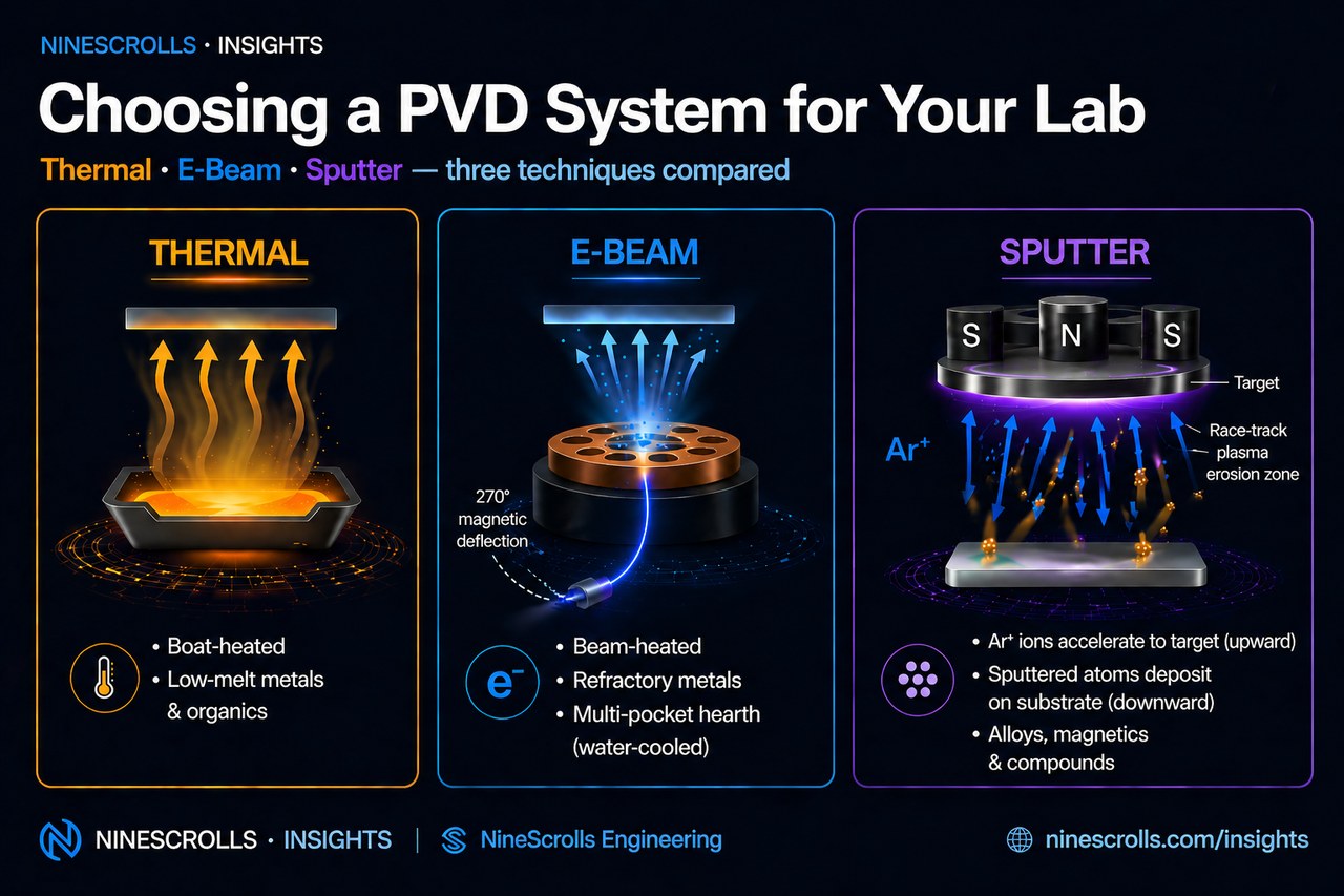
1) The Three PVD Techniques in 60 Seconds
All three techniques share a common premise: a source material is converted to vapor inside a high-vacuum chamber, and the vapor condenses onto a substrate to form a thin film. They differ in how the vapor is produced, and that difference cascades into every downstream property of the resulting film. The schematic in Figure 1 (below, after the spec table) illustrates each mechanism side by side — refer back to it as you read each technique.
1.1 Thermal Resistance Evaporation
A current of tens to hundreds of amperes is passed through a refractory-metal boat or basket holding the source material. Joule heating raises the boat to source-material sublimation temperature, and a vapor cloud rises through the chamber and condenses on the substrate. Because the boat itself is hotter than the source, contamination from the boat material (W, Mo, Ta) limits this technique to materials with melting points well below the boat's. It is the simplest and oldest PVD technique — first demonstrated in the 1880s — and still the right tool for evaporating Au, Al, Ag, In, organic semiconductors, and other low-temperature materials.
1.2 Electron Beam (E-Beam) Evaporation
A heated tungsten filament emits electrons that are accelerated through 6–10 kV and steered by a magnetic field into the source material sitting in a water-cooled copper crucible. The beam locally heats only the spot it strikes — typically to over 3000 °C — while the surrounding crucible stays near room temperature. This decouples the source from the crucible thermally and chemically, so even the most refractory materials (W, Mo, Ta, Pt, IrO2) can be evaporated without contamination from the holder. Modern e-beam guns include XY scanning to spread the beam across larger pockets and prevent crater drilling. Multi-pocket crucibles (typically 4–8 pockets, 7–25 cc each) let researchers load several materials and switch between them with a single rotation, enabling multi-layer optical stacks and lift-off metallizations in one pump-down.
1.3 Magnetron Sputtering
Instead of heating the source, sputtering uses momentum transfer. A negative bias of several hundred volts is applied to a solid target, which attracts argon ions from a low-pressure plasma. Each Ar+ impact ejects target atoms, which travel ballistically to the substrate. A magnetic field behind the target traps electrons close to the target surface, increasing the local plasma density and the sputter rate by an order of magnitude over plain DC sputtering. Because the source is never heated above a few hundred °C, the technique works for materials that decompose under thermal evaporation (oxides, nitrides, magnetic alloys) and for compound targets where stoichiometry must be preserved.
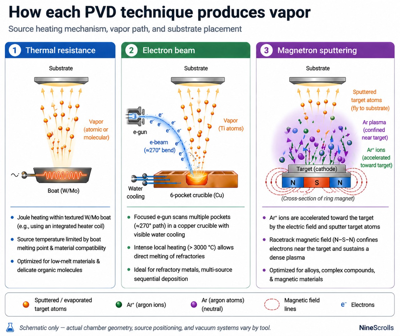
Figure 1: How each PVD technique produces vapor. Thermal heats a refractory boat by Joule heating; e-beam locally heats a copper crucible with a focused electron beam; sputtering ejects atoms from a target via Ar+ momentum transfer in a magnetron-confined plasma.
2) Core Trade-Offs at a Glance
The single most useful comparison for selecting a tool is the spec table below. Numbers are typical for research-grade systems on 4–8″ substrates — production tools push some of these further, but the relative ordering is stable across the industry.
| Property | Thermal | E-Beam | Magnetron Sputter |
|---|---|---|---|
| Max source temperature | ~1500 °C (boat-limited) | >3000 °C | N/A (momentum transfer) |
| Suitable materials | Low-melting metals, organics | Metals, oxides, nitrides, fluorides | Metals, alloys, oxides, nitrides, magnetics |
| Film purity | Medium (boat contamination risk) | Very high | High (depends on target purity) |
| Step coverage | Directional (line-of-sight) | Directional (line-of-sight) | More conformal |
| Lift-off compatibility | Excellent | Excellent | Marginal (sidewall coverage) |
| Stoichiometry control | Poor for compounds | Good for oxides; modest for alloys | Excellent |
| Typical deposition rate | 1–10 nm/s | 0.1–10 nm/s | 0.1–5 nm/s |
| Substrate damage | Very low (radiative heat only) | Low (some X-ray emission) | Moderate (energetic particles) |
| Multi-material in one run | Limited (one boat at a time) | Excellent (4–8 pocket crucibles) | Excellent (2–6 targets) |
| Capital cost (research grade) | $$ | $$$ | $$$–$$$$ |
| Footprint | Compact (~1 m2) | Medium (~1.5–2 m2) | Medium (~1.5–2 m2) |
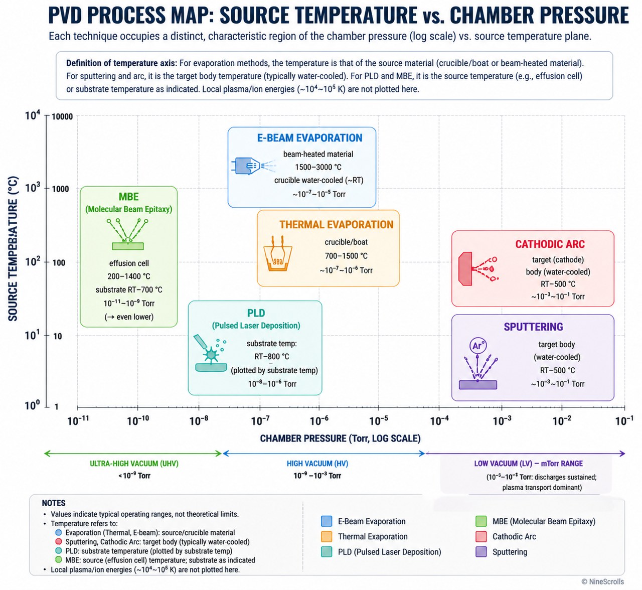
Figure 2: Operating regime map. The three techniques live in distinct corners of the (chamber pressure, source temperature) plane — e-beam reaches the highest source temperatures while staying in high vacuum; sputter trades vacuum for an Ar plasma at mTorr pressure; thermal sits between them at moderate temperature and HV.
3) Thermal Evaporation in Depth
3.1 When to Choose It
Thermal evaporation is the right tool when three conditions all hold: the source material melts well below 1500 °C, the substrate cannot tolerate energetic particle bombardment, and the budget or footprint cannot stretch to e-beam or sputter. Examples that fit this envelope cleanly: gold contacts on photodetectors, aluminum top electrodes on solar cells, indium bonding pads, silver mirrors on optical components, and the long list of organic small molecules used in OLEDs and OPVs (Alq3, NPB, PCBM, C60).
3.2 Where It Falls Short
The boat material sets the ceiling. A tungsten boat can heat a source to ~1800 °C before failing, but the W vapor pressure at that temperature is non-trivial, so films deposited near the boat's limit will pick up tungsten contamination. Refractory metals like W, Mo, Ta, Pt, and Pd are essentially un-evaporable thermally. Compound materials decompose: Al2O3 dissociates into Al and O, leaving you with sub-stoichiometric AlOx. Alloys fractionate — the lower-vapor-pressure component evaporates first, so the deposited film does not match the source composition over time. And because the boat is the hot zone, every run heats and fatigues the boat, so consumables cost is real ($20–$50 per run for high-quality boats in continuous use).
3.3 Practical Tips
- For lift-off, run at the lowest stable rate (0.5–2 nm/s) to keep substrate temperature low and avoid resist reflow.
- For Au, use a tungsten boat. For Al, use either a tungsten basket with a ceramic liner or a BN-coated boat — bare W reacts with molten Al.
- Always degas the source by ramping below evaporation temperature for 1–2 minutes before opening the shutter, otherwise the first nm of film will be rich in adsorbed contaminants.
- QCM (quartz crystal microbalance) thickness control is essential; rate fluctuations of ~10% are normal and need closed-loop power adjustment.
4) E-Beam Evaporation in Depth
4.1 When to Choose It
E-beam is the right tool when material purity matters, the source is refractory or a compound, or you need to deposit several materials sequentially in the same run. Typical applications: optical multilayer coatings (alternating SiO2/TiO2 for AR or HR), electron-transport layers in photodetectors (TiO2, SnO2), refractory contact metals (Ti/Pt/Au or Cr/Pt/Au stacks for III–V devices), MEMS structural layers, and IR optics on Ge, ZnS, or chalcogenide substrates. Recent published work using the MEB-600 e-beam evaporator includes a PbS microplate IR sensor in ACS Applied Materials & Interfaces (2024) and Ge/ZnS infrared photonic crystals in 2025.
A common misconception is that e-beam is only for refractory materials. It is perfectly capable of evaporating low-melting metals like Au, Al, and Ag — the difference is economic. Thermal evaporation of Au or Al is faster to set up, uses cheaper hardware, and runs at lower power. Choose e-beam for low-melt metals when one of three conditions applies: you need the multi-pocket crucible to deposit a stack including a refractory layer in the same run; you need the higher film purity that comes from a water-cooled crucible (no boat contamination); or your lab has only one tool and it must cover the full material range.
4.2 Where It Falls Short
E-beam is essentially line-of-sight. If your geometry has high-aspect-ratio trenches or sidewalls that need conformal coating, e-beam will leave shadowed regions uncovered — sputtering or ALD does this job better. Stoichiometry on alloys is intermediate: the more volatile component leaves the molten pool faster, so a long run drifts in composition. For fluorides and some oxides, the beam can dissociate the molecule on impact, leaving the film slightly oxygen-deficient unless an O2 backfill is used. Filaments are consumables (typically 100–500 hours of operation) and high-voltage power supplies need annual maintenance.
4.3 Practical Tips
- For refractory metals, use a graphite or fabmate liner inside the copper crucible to prevent alloy contamination from the Cu pocket walls.
- For oxides, expect 5–15% oxygen deficiency unless you backfill with 5–10 sccm O2 during deposition. Optical films almost always need this.
- XY beam scanning — horizontal (x) and vertical (y) raster deflection of the electron beam across the source pocket — is non-negotiable for pockets larger than ~10 mm. Without it, the stationary beam drills a crater that reduces the effective source area and rate over time. Tune the scan amplitude to fill ~70–80% of the pocket diameter and the scan frequency to a few hundred Hz so the molten pool stays uniform.
- Multi-pocket crucibles save days of process time on stack runs — never buy a single-pocket gun for a research lab unless the footprint is critical.
- Plan for in-situ QCM with endpoint detection. A standalone deposition without endpoint feedback is acceptable for thick films (>100 nm) but unacceptable for optical multilayers where 1 nm matters.
5) Magnetron Sputtering in Depth
5.1 When to Choose It
Sputtering wins when stoichiometry transfer matters most: alloy films where every atomic ratio must be preserved (CoFeB for spin-valve sensors, Ni80Fe20 for soft magnets, ITO transparent conductors), nitrides and oxides deposited reactively (TiN, AlN, Al2O3, ZnO), and applications that need large-area uniformity over a 6 or 8″ substrate. RF sputtering extends the technique to insulating targets (SiO2, glass, ceramics) that DC sputtering cannot drive. Multi-target tools enable co-sputtering for graded compositions.
5.2 Where It Falls Short
The same conformality that makes sputtering useful for trench filling makes it bad for lift-off — sidewall coverage of ~30–50% means resist sidewalls get coated, and the lift-off solvent cannot dissolve the photoresist underneath. Deposition rates are modest, so depositing >1 µm of film takes hours rather than tens of minutes.
Substrate damage is the trickier limit. Even "moderate" sputter conditions hit the substrate with 10–50 eV thermalised atoms, the occasional 100–500 eV sputtered ion, and reflected Ar neutrals plus stray UV photons from the plasma. That energetic flux is benign for Si, glass, and most epi semiconductors, but specifically harmful to:
- 2D materials (graphene, MoS2, WSe2) — even brief sputter exposure introduces vacancies, drops carrier mobility by 30–70%, and shifts photoluminescence peaks. Always deposit a thin (~5 nm) e-beam or thermal buffer first, then switch to sputter.
- Ultrathin gate oxides (HfO2, Al2O3 below ~3 nm) — sputter-deposited metals on top introduce trap states and can shift threshold voltage by hundreds of mV. ALD or e-beam contact metals are preferred.
- Organic device layers in OLEDs / OPVs / perovskite cells — the plasma UV degrades the emissive layer or absorbs into the active layer; never sputter directly onto a working organic stack without a sputter-buffer (typically thermal-evaporated MoOx or LiF).
- Flexible substrates (PET, PI, PEN) — thermal load and UV exposure can warp or yellow the substrate; pulse-mode and lower-power sputter mitigates but does not eliminate the issue.
Symptoms of damage on a finished device usually look like threshold-voltage shifts, mobility loss, increased dark current, or a reduction in photoluminescence yield — rarely visible on the wafer surface. If your device chemistry sits in this list, plan an evaporation step (e-beam or thermal) for the layer in direct contact with the sensitive surface, and reserve sputtering for upper metal interconnect and capping layers.
Finally, the chamber is harder to keep contamination-free than an evaporator. Sputter targets erode preferentially along the magnetron race-track, leaving a circular groove that eventually limits useful target life to ~30–50% of the slab thickness. Sputtered atoms also coat chamber walls, fixturing, and viewports, and that coating flakes off into particles over time. Routine wall cleaning, viewport polishing, and pump-line maintenance are part of the cost of ownership in a way they are not for evaporation.
5.3 Practical Tips
- Argon at 2–10 mTorr is standard. Lower pressure gives more energetic film growth (denser, more compressive stress); higher pressure gives more thermalised, more porous films.
- For reactive sputtering of oxides and nitrides, use closed-loop control on either O2 partial pressure or target voltage to avoid hysteresis between metallic and poisoned target modes.
- Substrate bias (RF or pulsed DC) tunes film density and stress — useful when you need a denser or more etch-resistant film.
- Pre-condition every new target by sputtering against a closed shutter for 5–10 minutes to remove the surface oxide layer. For reactive sputtering, also condition each time you switch between metallic and oxide / nitride modes — the target surface remembers its last poisoning state and the first minute of deposition will reflect that, not the steady-state composition.
- Magnetic targets (Fe, Co, Ni, FePt) erode unevenly because the magnetron field interacts with the magnetic target itself; rotate or replace at 30–50% of nominal life to maintain rate uniformity.
- Race-track erosion is normal. Track the depth weekly — once the groove approaches 60–70% of the slab thickness, plan a target swap before the magnetron magnets break through and damage the cathode.
6) Decision Matrix by Application
Working backward from what you actually want to deposit is faster than starting from the technique. The matrix below covers the most common research applications and the typical first-choice tool for each. "Hybrid OK" means the application is well-served by a multi-source platform like the MEB-600. Figure 3 visualises the same idea at a coarser, material-class level — useful for first-pass tool selection — and the decision flow in Figure 5 (see §9 below) condenses both into a two-question test for the most common cases.
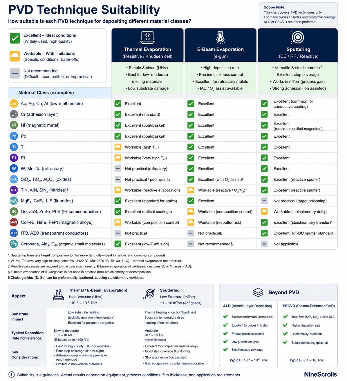
Figure 3: Material × technique suitability matrix. Green cells mark the typical first choice, yellow indicates a workable but non-optimal fit, gray means the technique is rarely the right answer for that class. Special-case applications (e.g. ALD for 3D conformal oxide) can override these defaults.
| Application | First choice | Notes |
|---|---|---|
| Lift-off Au or Al contacts (research) | Thermal or e-beam | Either works; thermal is cheaper, e-beam is more flexible |
| Lift-off Pt, Ti, Cr, W contacts | E-beam | Refractory; thermal not an option |
| Optical AR / HR multilayers (SiO2/TiO2) | E-beam (with O2 backfill) | Multi-pocket crucible saves run time |
| IR optics on Ge, ZnS, ZnSe | E-beam | Hybrid OK — published work uses MEB-600 |
| OLED / OPV organic layers | Thermal | Low temperature; e-beam decomposes most organics |
| UV down-conversion films on CMOS sensors | Thermal | Hybrid OK — published in JIMW using MEB-600 |
| ITO transparent electrodes | Sputter (RF) | Stoichiometry transfer essential |
| TiN or TaN diffusion barriers | Sputter (reactive) | Conformality wanted |
| CoFeB / NiFe magnetic layers | Sputter | Alloy stoichiometry, magnetic anisotropy |
| Si CMOS-compatible Al2O3 passivation | ALD (preferred) or sputter | Conformality on 3D structure |
| MEMS structural Cr / Ti sacrificial | E-beam | Lift-off compatibility plus high purity |
| Lift-off metal stacks for III–V devices | E-beam | Sequential layers, multi-pocket crucible |
7) Hybrid Systems: Why Most Research Labs Pick Two
Few labs can justify three separate PVD systems. The most common compromise is to pair sputtering (for compound and alloy films) with a multi-source evaporator that combines e-beam and thermal heads in one chamber. With this two-tool setup, a research group can cover more than 90% of typical thin-film deposition needs without compromising on any single technique.
The MEB-600 is one example of this hybrid approach: a single high-vacuum chamber houses a 6-pocket XY-scanned electron beam gun and thermal resistance boats, with in-situ quartz crystal monitoring and optional ion-source pre-clean. A single run can deposit a thermal Cr adhesion layer, an e-beam Pt contact, and a thermal Au capping layer without breaking vacuum — useful for lift-off processes and IR device fabrication. Paired with a magnetron sputtering system, the same lab handles compound films (TiN, Al2O3, ITO, magnetics) on the second tool.
For very large labs or production environments, dedicated single-purpose tools win on throughput and contamination control. For research environments where flexibility matters more than peak rate, the hybrid evaporator + sputter pair is hard to beat.
8) Cost of Ownership Beyond the Sticker Price
The capital cost of a research-grade PVD tool (~$80k–$300k depending on configuration) is rarely the dominant cost over a 5-year horizon. The recurring items typically add up to a comparable amount:
- Vacuum pumps. Turbo molecular pumps are typically rated for ~25 000 operating hours before bearing service or rebuild — that is 3–5 years at moderate research-lab use, ~12 months at 24/7 production use. A rebuild costs $3k–$8k depending on the pump model. The dry backing pump needs an oil-flush or tip-seal swap at 10 000–15 000 hours; budget $1k–$2k per service.
- Source consumables.
- Thermal: tungsten or molybdenum boats at $20–$50 each. Au boats last 50–100 runs; Al boats last only 5–15 runs because molten Al attacks the boat material. Plan on $200–$500/year for a moderately-used research tool.
- E-beam: filaments at $100–$300 each, with a typical service life of 100–500 operating hours. Filament life depends on the source material — oxides shorten life through filament oxidation, while pure metals are gentler. The high-voltage power supply and beam-deflection electronics need annual calibration ($500–$1500).
- Sputter: targets cost $500–$5000+ depending on size and material. Useful life ends at race-track depth of ~60–70% of slab thickness, which corresponds to ~50–200 hours of deposition for typical 3″ targets. Au and Pt targets are the cost outliers ($3k–$10k); aluminum, copper, and Si targets are cheap ($300–$800).
- Quartz crystal sensors. $30–$80 each, replaced when frequency drift exceeds tooling tolerance (typically 1–3 months of moderate use). Plan for one box of 10–20 crystals per year.
- Process gases. Sputtering uses Ar continuously; reactive sputtering adds O2, N2, or CH4. Evaporation systems use almost no gas in operation.
- Power. Sputter and e-beam pull 2–5 kW during deposition; thermal evaporation under 1 kW. Compounded over 24/7 operation in a multi-user facility, this is non-trivial.
- Cleanroom space. ~$500–$1500 per square meter per year in a typical academic cleanroom. A 2 m2 tool footprint is 2–3% of a moderate cleanroom's total cost.
- Service contracts. Optional but common for production tools; $5k–$20k per year. Less common for research tools that internal staff maintain.
For first-principles budgeting, plan on annual operating cost equal to roughly 10–15% of capital for a research tool with moderate use. A $150k e-beam system therefore costs ~$15k–$22k per year to keep running, before any process gases or staff time.
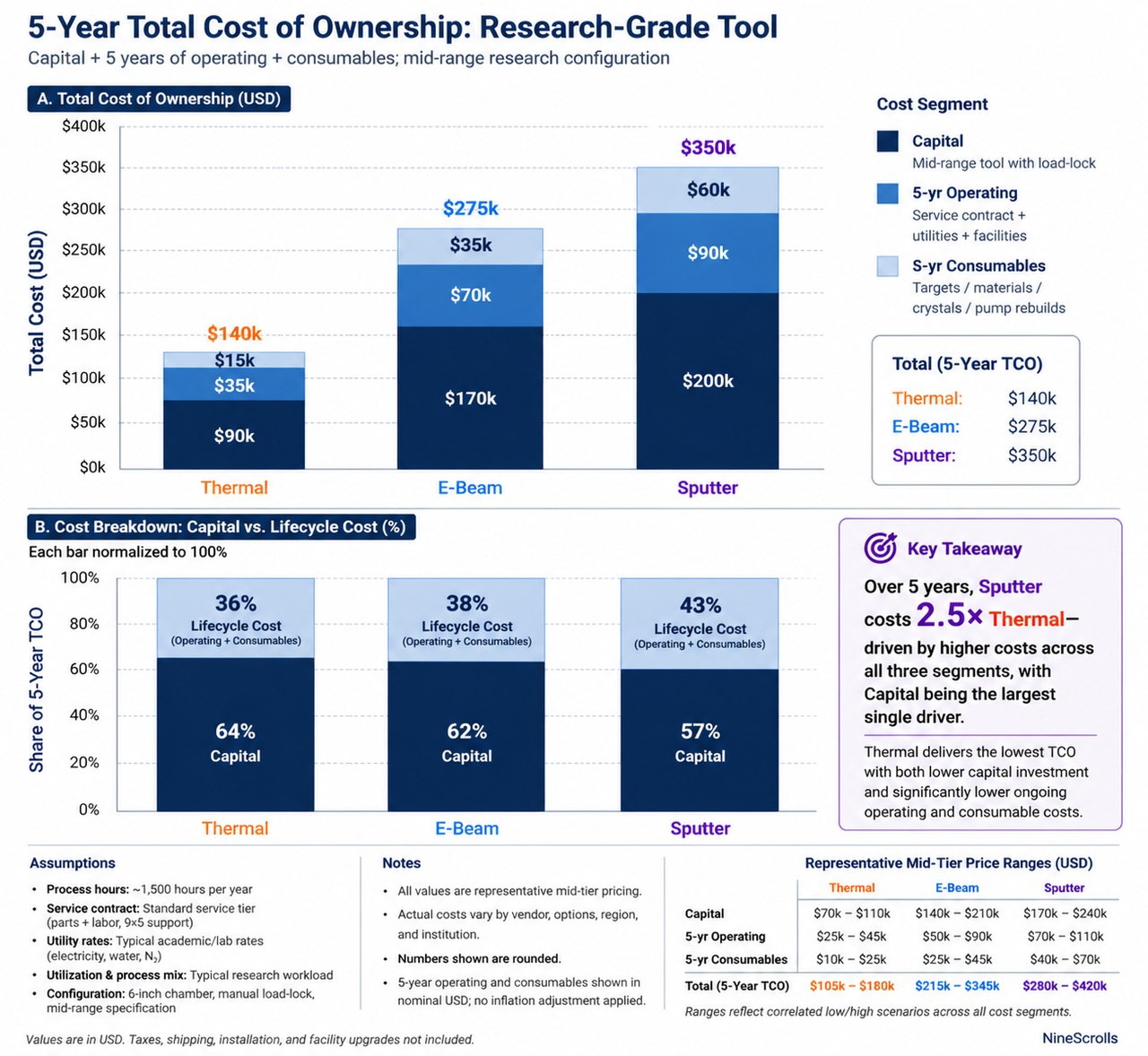
Figure 4: Five-year total cost of ownership for a mid-range research-grade tool. Thermal evaporation is the cheapest end-to-end; sputtering is the most expensive once consumables (targets) are factored in. E-beam sits between the two and is typically the best dollar-per-material-class value for a multi-purpose lab.
9) Conclusion: Pick the Tool That Matches Your Process
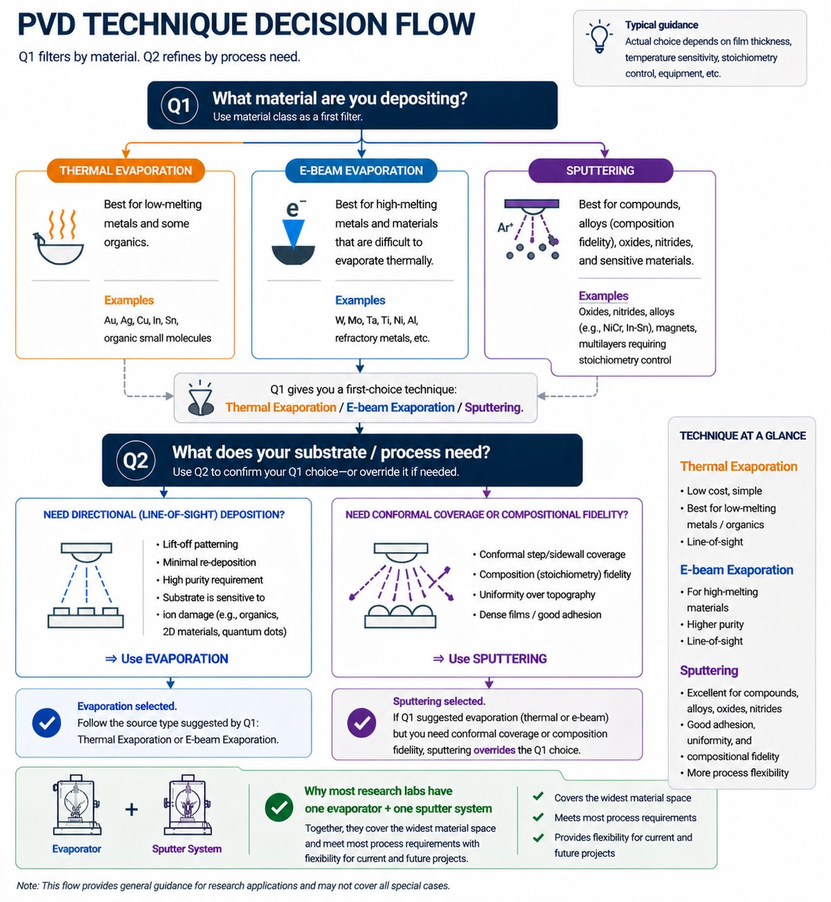
Figure 5: Two-question decision flow. The first cut is material type (thermal vs e-beam vs sputter), the second is substrate / process needs (evaporation for lift-off and purity, sputter for conformality and stoichiometry).
The right answer to "which PVD technique" almost always falls out of two questions:
- What are you depositing? Low-melting metals and organics → thermal. Refractory metals, oxides, fluorides, multilayers → e-beam. Alloys, magnetics, compound conductors and dielectrics → sputter.
- What does your substrate need? Lift-off and sensitive substrates → evaporation (thermal or e-beam). Conformal coverage and high stoichiometric fidelity → sputter.
If your roadmap covers both ends of either axis — for example, organic layers and refractory contacts — a multi-source evaporator like the MEB-600 covers both within one tool. Adding a sputter system on the side fills in compound films and conformal coatings. Most research-cleanroom buildouts converge on this two-tool combination after the first year, regardless of starting application.
Frequently Asked Questions
Can I deposit gold by sputtering instead of thermal or e-beam evaporation?
Yes, but it's almost never the right choice. Gold is easy to evaporate (melting point 1064 °C), so the conformality and substrate damage that come with sputtering are pure cost without benefit. The exception is when you need conformal Au coverage on 3D topography (e.g. coating MEMS structures from all sides) or when gold sticks better on a particular substrate after sputter pre-clean — then a sputter Au is worth considering. For flat-substrate lift-off contacts, thermal or e-beam is faster, cheaper, and gives a cleaner film.
Why does my e-beam SiO2 film come out absorbing or yellow?
Oxygen deficiency. The electron beam dissociates SiO2 molecules in flight, and some of the oxygen leaves the chamber before reaching the substrate. The result is sub-stoichiometric SiOx with x ≈ 1.7–1.9, which absorbs visible light. The fix is reactive deposition: backfill 5–10 sccm of O2 through a leak valve to maintain a partial pressure of ~1e-4 Torr during deposition. The film grows stoichiometric SiO2 and is optically clear in the visible. The same trick works for TiO2, Al2O3, and other oxide e-beam materials.
Is e-beam evaporation safe for sensitive electronic substrates like III–V epi or 2D materials?
Mostly yes, with one caveat. The e-beam itself stays inside the gun — what reaches the substrate is neutral vapor, plus a small amount of soft X-ray emission from the source (typically <10 keV). For Si, GaAs, GaN, and most epi structures, this is below the damage threshold. For 2D materials (graphene, MoS2) and ultra-thin oxide gate dielectrics, the X-ray dose can introduce trap states or charge accumulation. If your device shows post-deposition threshold shifts or mobility loss, switch to thermal evaporation (no X-rays) or interpose a sacrificial buffer layer. Sputtering, with energetic particle bombardment, is typically harder on these substrates than e-beam.
How important is QCM thickness control versus a simple time-and-rate recipe?
Critical for any film below ~100 nm or any multilayer where layer thicknesses set the optical or electronic response. Open-loop time-and-rate has 5–15% run-to-run variation due to source state, chamber pressure, and substrate temperature drift. A QCM with closed-loop power feedback brings that to under 2%, and an in-situ optical monitor on top of the QCM can hit 0.5% on optical multilayers. For thick mechanical or contact layers (>200 nm), open-loop is acceptable. For everything else, do not skip the QCM.
Can I sputter and evaporate in the same chamber?
Technically yes, and a few research clusters do bolt a sputter cathode onto an evaporator chamber. In practice the answer is almost always no — cross-contamination between source types, magnetic-field interference between the magnetron and the e-gun deflection, and the very different working pressures (mTorr for sputter, <1e-5 Torr for evaporation) make the combined chamber a compromise on both sides. The hybrid that does work cleanly is e-beam plus thermal evaporation in one chamber, since they share vacuum range and operating philosophy. For sputter capability, plan a second tool.
Do I need a load-lock for a research evaporator?
Strongly recommended for any tool with more than one user or shared between projects. A load-lock cuts pump-down time from 30–60 minutes to 5–10 minutes, increases throughput by 3–5x, and keeps the main chamber at base pressure between runs — which dramatically reduces water vapor contamination on the next sample. The cost adder is typically $15k–$30k for a single-wafer load-lock on a research tool, and it pays back inside a year for any multi-user facility.
NineScrolls PVD Equipment
NineScrolls supplies research-grade evaporation and sputtering systems for academic and industrial labs. The MEB-600 multi-source e-beam evaporator combines XY-scanned e-beam and thermal resistance sources in one chamber with a 6-pocket crucible and in-situ QCM endpoint — cited in ACS Applied Materials & Interfaces (2024). The Sputter System Series covers DC, RF, and magnetron configurations with 2–6 targets and substrate temperature up to 1200°C. Our applications team can review your target films, substrate, and throughput needs and recommend the right configuration for your lab.